Introduction
Current sensing is a critical function, necessary for precision closed-loop control in applications such as motor control, solenoid control, communications infrastructure, and power management. End uses range from safety-critical automotive and industrial applications to handheld devices, where power and efficiency are essential. Precision current monitoring allows designers to obtain critical instantaneous information, such as motor torque—based on motor current—efficiency of a dc-to-dc converter, or bias current in a base station's LDMOS (laterally diffused MOS) power transistor, or diagnostic information, such as shorts to ground.
To understand the key trade-offs, options, and challenges faced by system designers when choosing the most accurate, cost-effective current sensor for a circuit board, we take a close look at current sensing in LDMOS bias current monitoring in cellular base station power amplifiers and other relevant applications.
Current monitoring is necessary in base station power amplifiers, especially with the more complex modulation methods used in 3G and LTE, where the peak-to-average power ratio varies from 3.5 dB (about 2.2 to 1) for 3G W-CDMA to 8.5 dB (about 7.1 to 1) for LTE OFDM—compared with 3 dB (about 2 to 1) for the most popular 2G single-carrier GSM. One of the control-loop functions is to monitor the LDMOS bias current, which allows the bias of the LDMOS to be properly modulated for a given power output. Typically, this dc bias current has a wide dynamic range based on operating, maximum, or off-peak operation. To the designer, this means that an accurate current sensor is needed to monitor a current that can range from 50 mA (or as little as 15 mA)1 to 20 A, while the drain of the LDMOS is biased at a high voltage ranging from 28 V to 60 V. Using a shunt resistor to monitor this current means that the designer is limited to a very small shunt that will not dissipate too much power when the LDMOS current is 20 A. As an example, even a 10 mΩ shunt will dissipate 4 W at maximum current.
While shunt resistors are available to handle this power, lower power dissipation might be a requirement of the board. But the choice of such low resistance values means that at low currents, say 50 mA, the voltage across the 10 mΩ shunt is extremely small (500 μV), making it a challenge to monitor accurately—with a circuit that must also withstand high common-mode voltage.
This article will focus on providing current-sensing solutions that can help designers accurately monitor wide-ranging dc currents in the presence of high common-mode voltages. Special attention will also be devoted to temperature performance, a critical parameter that is often not easy to calibrate but must be faced in the case of outdoor power amplifiers. Three optional solution approaches are described here—in order of decreasing design complexity—that provide viable high-accuracy, high-resolution current sensing for a variety of applications.
- Use discrete components, such as op amps, resistors, and Zener diodes, to build a current sensor. This solution employs the AD8628 zero-drift amplifier as its key component.
- Attain an increased level of integration by using a high voltage bidirectional current shunt monitor, such as the AD8210, with additional external components to extend dynamic range and accuracy.
- Employ an application-optimized device such as the newly available AD8217, an easy-to-use, highly integrated zero-drift current sensor with an input common-mode voltage range of 4.5 V to 80 V.
Configuring a Standard Op Amp for High-Side Current Sensing
Figure 1 shows an op-amp-based discrete solution employing the AD8628. The same setup is valid with other op amps as well, but specific features that are required include low input offset voltage, low offset voltage drift, low input bias current, and rail-to-rail input- and output swing capability, if possible. Other recommended amplifiers include the AD8538, AD8571, and AD8551.

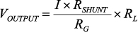
This circuit monitors the high-side current, I. The amplifier is biased on via the Zener diode, which, in this case, is rated at 5.1 V. Its use ensures that the amplifier operates safely at the high common-mode level and that its supply voltage remains steady and within the allowed supply limits, while the output is converted to a current by the MOSFET—and to a ground-referenced voltage by resistor RL. The output voltage can thus feed converters, analog processors, and other ground-referenced components—such as op amps or comparators—for further signal conditioning.
In this configuration, the voltage across RG is equal to the voltage across RSHUNT because feedback via the MOSFET maintains both high-impedance op-amp inputs at the same voltage. The current through RG flows through the FET and RL to develop VOUTPUT. The relationship between the current, I, flowing through the shunt resistor and VOUTPUT is expressed by Equation 1:
 |
(1) |
RSHUNT Selection: The maximum value of RSHUNT is limited by the allowable power consumption at maximum current. The minimum value of RSHUNT is limited by the input range and error budget of the op amp. Normally, the value of RSHUNT is from 1 mΩ to 10 mΩ for monitoring currents greater than 10 A. If a single resistor cannot meet the power consumption requirement or is too large for the PCB, RSHUNT may have to be made up of multiple resistors in parallel.
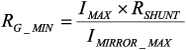
RG Selection: RG is used to translate a current proportional to the high-side current to the low-side. The maximum RG is limited by the drain-source leakage current of the P-channel MOSFET. For example, consider the common P-channel enhancement-mode vertical DMOS transistor BSS84. The maximum IDSS at various conditions is shown in Table 1.
Table 1. Drain-Source Leakage Current
| Conditions | Maximum IDSS |
| VGS = 0 V; VDS = –40 V; TJ = 25°C | –100 nA |
| VGS = 0 V; VDS = –50 V; TJ = 25°C |
–10 µA |
| VGS = 0 V; VDS = –50 V; TJ = 125°C | –60 µA |
Consider the LDMOS drain current monitoring example, with 28-V common mode and IDSS of 100 nA. The mirror of the minimum current through RL should be at least 20 times IDSS. This results in
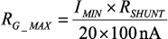
The minimum RG is limited by allowable mirror current power consumption at maximum load current
RBIAS Selection: The current through RBIAS divides to produce the op amp's quiescent current and the essentially constant Zener-diode voltage, VZ, (which determines the op amp's supply voltage). Make sure the current flowing through the Zener diode does not exceed its maximum regulated current, IZ_MAX, when the amplifier current, ISUPPLY, is essentially zero and VIN is the maximum:
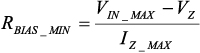
To ensure a stable diode voltage, the current flowing through it should be higher than its minimum operating current, IZ_MIN, when ISUPPLY is the maximum and VIN is the minimum:

The Zener diode and RBIAS are the key components in this solution because they take away the high common-mode voltage from the following circuits and allow the use of a low-voltage precision op amp. For best voltage stability, the Zener diode should have low dynamic resistance and low temperature drift.
R1 Selection: R1 is used to limit the amplifier input current if input transients exceed the op amp's power supply voltage. A 10-kΩ resistor is recommended.
The offset voltage, VOS, and offset current, IOS, of the chosen op amp are critical, especially with low values of shunt resistance and at low load currents. VOS + IOS × R1 must be smaller than IMIN × RSHUNT, or the amplifier may be saturated. Therefore, a rail-to-rail input amplifier with zero crossover distortion is preferred for optimal performance.
Another issue to consider for this discrete solution is temperature drift. Even if an amplifier with zero drift is used, it is very difficult or costly to optimize drifts caused by discrete components: the Zener diode, MOSFET, and resistors. From Table 1, the maximum IDSS of the MOSFET changes from –10 μA to –60 μA as the operating temperature changes from 25°C to 125°C with VGS = 0 V and VDS = –50 V. This drift will degrade the system accuracy over temperature, especially when the monitored current is low. The drift of the Zener diode will impact the stability of the amplifier's power supply, so the amplifier used should have high power-supply rejection (PSR).
Further, designers must take into account the low power efficiency of this solution: A lot of power is consumed by RBIAS. For example, if the bus common-mode voltage is 28 V, the Zener-diode voltage output is 5.1 V, and RBIAS is a 1000-Ω resistor, the circuit will dissipate more than 0.52 W of undesirable power. This adds to the power-consumption budget and must be taken into account.
High-Side Current Sensing with the AD8210 and External Components
Figure 2a shows a simplified block diagram of the AD8210 integrated high-voltage bidirectional current shunt monitor; Figure 2b shows a unidirectional application with an external voltage reference.
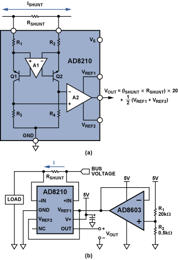
(b) Wide-range unidirectional application with an external reference.
The AD8210 amplifies a small differential input voltage generated by a positive or negative current flowing through the shunt resistor. The AD8210 rejects high common-mode voltages (up to 65 V) and provides a ground-referenced buffered output.
As shown in Figure 2a, it comprises two main blocks, a differential amplifier, and an instrumentation amplifier. The input terminals are connected to differential amplifier A1 via R1 and R2. A1 nulls the voltage appearing across its own input terminals by adjusting the small currents through R1 and R2 with Q1 and Q2. When the input signal to the AD8210 is 0 V, the currents in R1 and R2 are equal. When the differential signal is nonzero, the current increases through one of the resistors and decreases in the other. The current difference is proportional to the size and polarity of the input signal.
The differential currents through Q1 and Q2 are converted into a differential voltage by R3 and R4. A2 is configured as an instrumentation amplifier. The differential voltage is converted into a single-ended output voltage by A2. The gain is internally set to 20 V/V with precision-trimmed, thin film resistors.
The output reference voltage is easily adjusted using the VREF1 and VREF2 pins. In a typical configuration for handling bidirectional current flow, VREF1 is connected to VCC while VREF2 is connected to GND. In this case, the output is centered at VCC/2 when the input signal is 0 V, so with a 5-V supply the output is centered at 2.5 V. The output will be greater or less than 2.5 V, depending on the direction of the current through the shunt resistor.
This configuration works well for charge/discharge applications, but if the user needs to utilize the entire output range to measure a unidirectional current flow, then the circuit of Figure 2b shows a typical way that an external source may be used to set the range. Here a resistive divider is buffered by an op amp to drive the VREF1 and VREF2 pins, connected together, to offset the output.
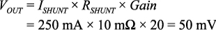
It is difficult for the amplifier alone to monitor the load current as it comes close to zero. With a 5-V supply, the AD8210 specifies a linear output range with a minimum output of 50 mV and a maximum output of 4.9 V. Consider an application where the shunt resistance is 10 mΩ. The minimum current through it must be greater than 250 mA to ensure that the output of the AD8210 is above its lowest point of 50 mV.
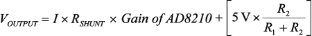
The configuration shown in Figure 2b adds an offset to allow smaller currents to be measured. The relationship between output voltage and monitor current, based on an amplifier gain of 20 V/V, can be calculated as Equation 2:
 |
(2) |
For example, using resistances, R1 and R2, of 9800 Ω and 200 Ω, respectively, the offset voltage will be 100 mV. When the differential input is 0 V, the AD8210 output will now be 100 mV, safely in the linear range. If the range of shunt current is from 50 mA to 20 A, with RSHUNT = 10 mΩ, the input range would be 0.5 mV to 200 mV; and the output range of the AD8210 is 10 mV to 4 V plus the offset voltage, or 0.11 V to 4.1 V, well within the AD8210's specified linear range.
In fact, using this configuration, the designer can offset the output of the AD8210 to any point within its supply range in order to handle arbitrary current ranges having any degree of asymmetry. An op amp to buffer the voltage divider is desirable because precision-trimmed resistances are connected internally to the reference inputs—so, for best results, those inputs should be driven at low impedance. Precision and low cost op amps that can be used to buffer the external reference include—for example—the AD8541, AD8601, AD8603, AD8605, AD8613, AD8691, and AD8655.
Compared with the discrete solution, this integrated solution requires that the current shunt monitor have high common-mode voltage range and an output offset—if the output voltage range cannot meet the current-detection range requirements. But it can handle bidirectional current monitoring, and it avoids the temperature drift and power consumption issues described above. The offset drift and gain drift of the AD8210 are guaranteed to be a maximum of 8 µV/°C and 20 ppm/°C, respectively. And if, for example, the AD8603 were used as the buffer, it would contribute an offset of only 1 µV/°C, which can be neglected compared with the AD8210's already low offset-voltage drift. The power consumption of the divider, R1 and R2, is

or only 1.2 mW, using the parameters in Figure 2b.
High-Side Current Monitoring Using the Zero-Drift AD8217
Recently, Analog Devices introduced the AD8217, a high-voltage current sensor featuring zero drift and 500-kHz bandwidth, designed specifically to enhance resolution and accuracy over wide temperature-, input common-mode-, and differential voltage ranges. Figure 3a shows a simplified block diagram of the device; Figure 3b shows it in a typical application.

(b) High-side current sensing using the AD8217.
For measuring very small currents through a small shunt resistor, the AD8217 features a minimum 20-mV output range over temperature, an improvement over the AD8210's 50-mV range. Thus, if the minimum load current being monitored across the shunt produces 20-mV minimum output, which is 1-mV minimum input, from the current sensor, then the user can choose the AD8217 configured as shown in Figure 3b. The relationship between the output voltage of the AD8217 and the input current can be calculated as Equation 3:
 |
(3) |
The AD8217 features an internal low-dropout regulator (LDO), which provides a constant-voltage supply to the amplifier. The LDO withstands the high common-mode voltage that can vary from 4.5 V to 80 V, essentially performing a similar function to that of the Zener diode in Figure 1.
The AD8217 features a factory-set gain of 20 V/V, with a maximum ±0.35% gain error over the entire temperature range. The initial offset, specified ±300 µV over temperature, and the miniscule temperature drift, ±100 nV/°C, will enhance any error budget. The buffered output voltage directly interfaces with any typical analog-to-digital converter. Regardless of the common mode, the AD8217 provides the correct output voltage when the input differential is at least 1 mV. Using a 10-mΩ shunt resistor, as above, the minimum current can be as low as 100 mA.
The single-chip solution avoids the temperature drift and power consumption issues of the discrete solution.
Performance Results Compared
The following section will display test results obtained comparing the three different methods. The input current through the shunt was adjusted by changing both the input voltage and load resistance. In the data, initial calibration has been performed in order to remove the initial gain and offset errors associated with all the parts used in our board.
Figure 4 is a linearity plot of the output voltage across RL as a function of low-end values of input current flowing through RSHUNT, measured using the circuit of Figure 1. RSHUNT is 10 mΩ; RG is 13 Ω; RBIAS is 100 Ω; R1 is 10 kΩ; load resistance is 200 Ω; RL is 200 Ω; the Zener diode output is 5.1 V; the op amp is AD8628; the MOSFET is BSS84. The maximum relative error is 0.69%, and the average is 0.21% after calibration.
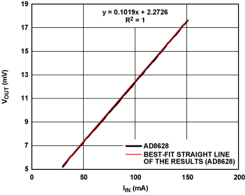
Figure 5 is a linearity plot of the output voltage of the AD8210 as a function of low-end values of input current flowing through RSHUNT, measured using the circuit of Figure 2b. RSHUNT is 10 mΩ; R1 is 20 kΩ; R2 is 0.5 kΩ; the load resistance is 200 Ω. The external reference buffer is an AD8603. The maximum relative error is 0.03%, and the average is 0.01% after calibration.
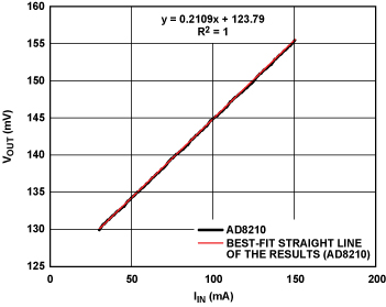
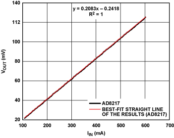
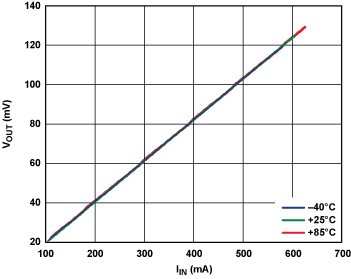
Figure 6 is a linearity plot of the output voltage of the AD8217 vs. low-end values of input current flowing through RSHUNT in the circuit of Figure 3b. RSHUNT is 10 mΩ, and the load resistance is 50 Ω. The maximum relative error is 0.088%, and the average is 0.025% after linear correction.
Note that the tests were necessarily concentrated at the low end of the range and did not cover the full 50 mA to 20 A range. The reason is that the linearity challenge is mainly at the low output voltage (low unipolar current) portion of the range.
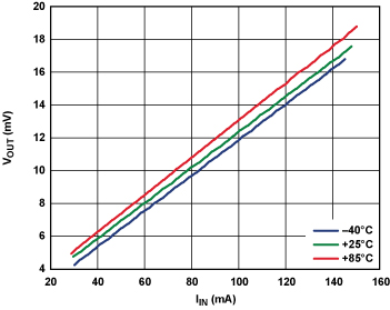
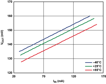
Temperature experiments were also done for each solution at –40°C, +25°C, and +85°C. Table 2 shows the maximum relative error and average error when using the same correction factor at +25°C to calibrate the data at –40°C and +85°C.
Table 2. Maximum and Average Error at Different Temperatures Using the Same Correction Factor
| Solution Circuit | AD8628 |
AD8210 | AD8217 |
|
| –40°C | Max error (%) |
11.982 |
2.117 | 0.271 |
| Avg error (%) |
4.929 |
2.059 |
0.171 | |
| +25°C | Max error (%) | 1.806 | 0.075 | 0.103 |
| Avg error (%) | 0.228 | 0.039 | 0.022 | |
| +85°C | Max error (%) | 6.632 | 3.800 |
0.918 |
| Avg error (%) | 5.769 |
3.498 |
0.421 | |
If a temperature sensor is available for use in the system, different correction factors can be used to calibrate the data at different temperatures, but with increased component and manufacturing cost. Table 3 shows the maximum relative error and average error when different correction factors are used at –40°C, +25°C, and +85°C.
Table 3. Maximum and Average Error at Different Temperatures Using Different Correction Factors
| Solution Circuit | AD8628 |
AD8210 | AD8217 |
|
| –40°C | Max error (%) |
1.981 |
0.022 | 0.114 |
| Avg error (%) |
0.303 |
0.009 |
0.023 |
|
| +25°C | Max error (%) | 1.806 | 0.075 | 0.103 |
| Avg error (%) | 0.228 | 0.039 | 0.022 | |
| +85°C | Max error (%) | 1.844 | 0.038 |
0.075 |
| Avg error (%) | 0.241 |
0.013 |
0.020 | |
The temperature experiments show the high accuracy available over wide temperature ranges with devices using auto-zero technology, especially in the case of the AD8217.
Conclusion
The test results show that all three solutions can be used for wide dynamic range high-side current sensing: the outputs are linear in all three solutions, while the solution using the AD8217 leads to the best error performance without the necessity of a standalone power supply. The ±100-nV/°C offset drift characteristic also makes it ideal for the most accurate performance throughout the –40°C to +125°C temperature range. From a system design perspective, the single-chip solution can save PCB area, ease PCB layout, decrease system cost, and improve reliability. These findings apply particularly to unidirectional current sensing applications, where the load-current range is wide and dynamic range is critical.
Based on these test results, the AD8217 solution is the most suitable of the three choices for wide dynamic range unidirectional high-side current sensing and monitoring. We also note that an AD8210 solution offers operation right down to 0-V inputs—which could be beneficial for short-to-ground conditions. Note also that the AD8210 is capable of single-chip monitoring of bipolar current flow, as in charge/discharge applications.
Calibration and temperature sensing are recommended in practical system designs requiring best system performance.
Acknowledgements
Mr. Ryan Du contributed to the discrete solution setup and measurement portion of this article while interning at Analog Devices.
1According to Antenna Interface Standards Group (AISG) 1.1.


