Reference Design for the MAX5073 Dual Buck Converter Operating at a Switching Frequency of 2MHz
Description
This article shows a detailed reference design using the MAX5073 as a dual buck converter with a switching frequency of 2MHz. This design can be used in applications that are space limited, because the higher switching frequency allows smaller passive components to be used on the board. In addition, this power solution can be used (in conjunction with load-dump protection) for automotive applications that require a switching frequency outside of the AM radio band, such as those found in automotive instrument clusters and infotainment systems.
Key specifications for this reference design are listed below, along with a detailed schematic (Figure 1) and the bill of materials (Table 1) needed for this application.
Specifications:
- Input Voltage: 5.5V to 16V
- Converter 1 Output Voltage = 3.3V/2A (max)
- Converter 2 Output Voltage = 2.5V/1A (max)
- Switching Frequency (fSW) of Each Converter = 2MHz
- Temperature with Airflow (TA) = -40°C to +85°C

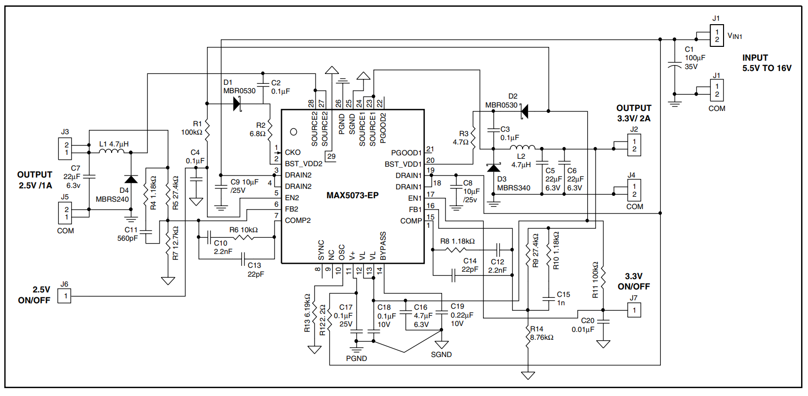
| Designator | Value | Description | Part | Footprint | Manufacturer | Quantity |
| C1 | 100µF/35V | Capacitor | EEVFK1V101P | 8mm x 10.2mm | Panasonic | 1 |
| C2, C3, C4, C17, C18 | 0.1µF/25V | Capacitors | GRM188R71E104KA01D | 603 | Murata | 5 |
| C5, C6, C7 | 22µF/6.3V | Capacitors | GRM31CR60J226KE19 | 1206 | Murata | 2 |
| C8, C9 | 10µF/25V | Capacitors | GRM31CR61E106KA12 | 1206 | Murata | 1 |
| C10, C12 | 2.2nF | Capacitors | GRM188$71H222JA01 | 603 | Murata | 2 |
| C11 | 560pF | Capacitor | GRM188R71H561KA01 | 603 | Murata | 1 |
| C13-C14 | 22pF | Capacitors | GRM1885C1H220JA01 | 603 | Murata | 2 |
| C15 | 1nF | Capacitor | GRM18871H102KA01 | 603 | Murata | 1 |
| C16 | 4.7µF/6.3V | Capacitor | GRM188R60J475KE19B | 603 | Murata | 1 |
| C19 | 0.22µF/10V | Capacitor | GRM188R71A224KA01 | 603 | Murata | 1 |
| C20 | 0.01µF | Capacitor | GRM188R71H103KA01J | 603 | Murata | 1 |
| D1, D2 | 30V, 500mA | Schottky Diodes | MBR0530 | SOD123 | ON Semiconductor | 2 |
| D3 | 40V, 3A | Schottky Diode | MBRS340 | SMC | ON Semiconductor | 1 |
| D4 | 40V, 2A | Schottky Diode | MBRS240 | SMB | ON Semiconductor | 1 |
| L1, L2 | 4.7µH | Inductors | IHLP2525-CZ | 6.86mm x 6.47 mm x 3.18 mm | Vishay | 1 |
| R1, R11 | 100kΩ | Resistors | SMD, 1%, 0.125W | 603 | Vishay | 2 |
| R2 | 6.8Ω | Resistor | SMD, 1%, 0.125W | 603 | Vishay | 2 |
| R3 | 4.7Ω | Resistor | SMD, 1%, 0.125W | 603 | Vishay | 1 |
| R4, R8, R10 | 1.18kΩ | Resistors | SMD, 1%, 0.125W | 603 | Vishay | 3 |
| R5, R9 | 27.4kΩ | Resistors | SMD, 1%, 0.125W | 603 | Vishay | 2 |
| R6 | 10kΩ | Resistors | SMD, 1%, 0.125W | 603 | Vishay | 1 |
| R7 | 12.7kΩ | Resistors | SMD, 1%, 0.125W | 603 | Vishay | 1 |
| R12 | 2.2Ω | Resistor | SMD, 1%, 0.125W | 603 | Vishay | 1 |
| R13 | 6.19kΩ | Resistor | SMD, 1%, 0.125W | 603 | Vishay | 1 |
| R14 | 8.76kΩ | Resistors | SMD, 1%, 0.125W | 603 | Vishay | 1 |
| U1 | MAX5073 | Dual Buck Converter | MAX5073ETI+ | 32-TQFN_EP (5mm x 5mm) | Maxim | 1 |
Actual measurements taken from the board showing the efficiency performance are shown in Tables 2 and 3.
| VIN (V) | IIN (A) | VOUT1 (V) | IOUT1 (A) | Efficiency (%) |
| 14.007 | 0.065732 | 3.3371 | 0.1018 | 36.8973373 |
| 14.010 | 0.183690 | 3.3339 | 0.5122 | 66.3542117 |
| 14.005 | 0.267750 | 3.3321 | 0.8032 | 71.3722082 |
| 14.007 | 0.329490 | 3.3309 | 1.0112 | 72.9812485 |
| 14.005 | 0.449290 | 3.3298 | 1.4007 | 74.1230723 |
| 14.002 | 0.584520 | 3.3281 | 1.8203 | 74.0201375 |
| 14.001 | 0.650260 | 3.3267 | 2.0150 | 73.6279304 |
| VIN (V) | IIN (A) | VOUT2 (V) | IOUT2 (A) | Efficiency (%) |
| 14.008 | 0.044533 | 2.5350 | 0.1075 | 43.6845979 |
| 14.008 | 0.044533 | 2.5350 | 0.1075 | 43.6845979 |
| 14.008 | 0.067144 | 2.5337 | 0.2049 | 55.1967881 |
| 14.003 | 0.087638 | 2.5337 | 0.3010 | 66.3986847 |
| 14.005 | 0.133680 | 2.5337 | 0.5122 | 69.3178710 |
| 14.005 | 0.155350 | 2.5338 | 0.6097 | 71.0058542 |
| 14.008 | 0.255976 | 2.5334 | 1.0001 | 70.6596037 |
In terms of stability, bode plots for each output are shown in Figures 2 and 3, detailing the gain and phase of each output.
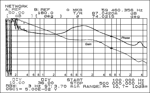
Figure 2. Bode plot for a VOUTPUT of 3.3V/1.4A
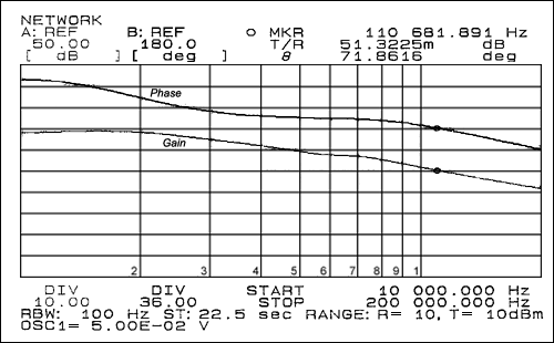
Figure 3. Bode plot for a VOUTPUT of 2.5V/0.6A
この記事に関して
最新メディア 21