要約
Consider a scenario that is all too common: Far along in the process of developing a peripheral that will interface with the USB port of a PC, the designer takes up the problem of how it should be powered. This power source can pose a problem, because the peripheral must operate when the PC is shut down as well as when it is up and running.
It makes sense to obtain power from the PC's USB port, but that approach allows operation only when the PC is running. Another obvious solution is a standard 110VAC outlet and an ac-dc converter, but that source exposes the device to the noise and voltage fluctuations inherent in any ac outlet. Thus, an alkaline or rechargeable battery, though not practical as the sole power source, is a necessary component if the peripheral is to be portable. A third option is to make use of all three power sources. Though sacrificing simplicity, that arrangement makes the product more versatile, and it is not as difficult or as costly as one might think.
Circuitry for switching between the adapter and USB portcan be as simple as a MOSFET and diode, or as complex as two power converters. Either case requires a battery, both for backup and to enable portable operation. The following discussion introduces different ways to utilize the advantages of all three power sources. Each option has pros and cons, but each gets the job done.
Dirt Cheap
A diode, a FET, and a resistor are all it takes to build a basic switchover circuit. The input stage of Figure 1 shows how the circuit accomplishes seamless switching between the USB port and the adapter. As voltage on the USB supply line drops, the FET connects the +5V adapter to the battery charger. Under a load of 250mA, this connection occurs when the USB voltage drops to +4.3V.
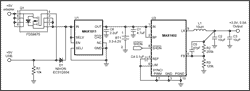
Figure 1. This simple circuit accomplishes power-supply switchover with seamless switching, but runs the risk of connecting both supplies at once.
A low component count makes this topology quite reliable, and also simplifies any necessary debugging and failure analysis. The circuit provides +1.25V to +5V at up to 600mA, with 95% efficiency. The backup battery ensures that this output is immune to power supply noise and droop. And just in case the device is to be non-portable, the switchover is fully functional without the battery.
The battery charger functions only with input voltages in the range +4.35V to +6.5V. When its supply voltage falls below +4.35V, as is possible when switchover is attempted under load, the battery charger disconnects from the battery completely, leaving only the battery to supply the load. This circuit may not switch cleanly when the adapter voltage is low. Unless the FET is turned off with a 0.5V threshold, it conducts slightly and allows the battery to discharge through that connection to the adapter input. A simple way to alleviate this concern is to put a diode in series with the adapter, thereby eliminating the possibility of reverse currents.
A Bit More
Though slightly more complex, the circuit of Figure 2 functions much the same way as that of Figure 1. Instead of one FET connecting adapter and battery charger when the USB voltage drops, this circuit includes three FETs, a voltage detector, and an inverter to ensure connection at a specific switchover point.
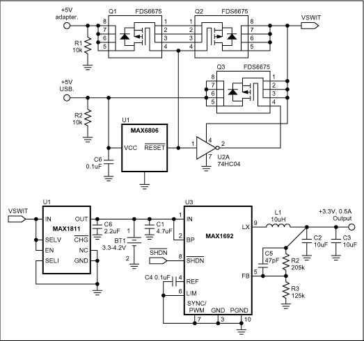
Figure 2. To retain the advantage of seamless switching while eliminating the possibility of connecting both supplies at once, substitute a MOSFET for the diode in Figure 1 and add a voltage detector (U1) and inverter (U2). The resulting circuit allows the designer to set a precise switchover point.
Because the designer can configure the voltage detector (U1) to switch at different voltages, any drop in voltage seen during the switchover can also be defined by the designer. When U1's VCC falls below an internal reference voltage, active-low RESET goes low and immediately turns on Q1 and Q2. Q3 is immediately turned off by U2A, whose input is the active-low RESET line. To protect the associated components from reverse current and to ensure continuous power to the load, the inverter's fall time ensures that both supplies are connected for a maximum of only 500ns. As for Figure 1, this circuit provides +1.25V to +5V at up to 600mA, with 95% efficiency. The battery ensures output immunity to power supply noise and droop, and for non-portable designs the switchover is fully functional without the battery.
Precise switching from USB input to adapter input obviates the need for close regulation of the inputs, and also enables the designer to determine the level of acceptable droop. Back-to-back FETs on the secondary input enables the circuit to block reverse currents that could otherwise flow from the battery to either input. The FETs also guard against the effect of any potential difference between the USB input and adapter input.
The presence of a voltage detector and FET on the primary input and two FETs on the secondary input adds to circuit complexity and relative cost, and makes this circuit more difficult to debug. The two FETs also drop the input voltage approximately 0.3V more than the single FET of Figure 1, which reduces efficiency from the USB and adapter inputs. Again, the battery charger functions only for input voltages in the range +4.35V to +6.5V.
Top of the Line
Let's suppose the peripheral in question is a global positioning system (GPS) that operates in a car after the user downloads a map from their PC. Circuitry that allows switchovers between more than one source voltage is critical. Figure 3 shows a robust and versatile power-supply/switchover circuit that offers many advantages over the circuit designs just discussed.
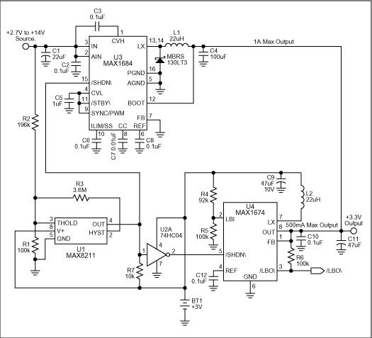
Figure 3. The use of stepup and stepdown converters (U3 and U4) enables this circuit to maintain all the advantages of Figure 2 while operating at a higher level of efficiency.
The input range of dc-dc stepdown converter U3 (+2.7V to +14V) allows connection to a variety of sources. Two useful examples include a USB port and a 12V automobile source. U3 delivers up to 1A of output current for output voltages ranging from +1.25V to +14V, with efficiency as high as 96%. With no USB or adapter voltage present, the voltage detector and inverter (U1 and U2) ensure switchover to the dc-dc stepup converter (U4), which operates from a battery with efficiency as high as 94%. U4 delivers up to 500mA for outputs from +2V to +5.5V. That flexibility allows a user to download information to a device, unplug it from a primary power source, carry it to a car or other power source and plug it back in, all without interruption of operation.
One limitation of U4 is that it cannot support operation if you disconnect the circuit from the USB or adapter source while drawing a load current greater than 500mA. U4's output voltage will drop and the load will shut down. Moreover, the absence of a battery charger in the circuit requires the user to replace batteries periodically. (As an alternative, you can simply add a charger and rechargeable batteries.)
Fully Integrated
A single IC (Figure 4) provides a fully integrated circuit that minimizes board space and enables many power-source options. The MAX1774 contains two high-efficiency stepdown converters with battery-backup switchover. It provides two output voltages derived from either an external power source or a main battery. The main output voltage is adjustable from +2.6V to +5.5V, and delivers over 2A of load current with efficiency up to 95%. The core output is adjustable from +1V to +5V, and delivers load currents up to a 1.5A with efficiency up to 91%. If neither the USB nor the adapter input is active, the main battery supplies both outputs at these high efficiencies. If the main battery then runs low, circuitry internal to the MAX1774 switches the load to a backup battery. The IC's input range (+2.7V to +28V) allows it to be powered by a standard 110V-to-5V ac-dc converter or the +12V supply of an automobile.
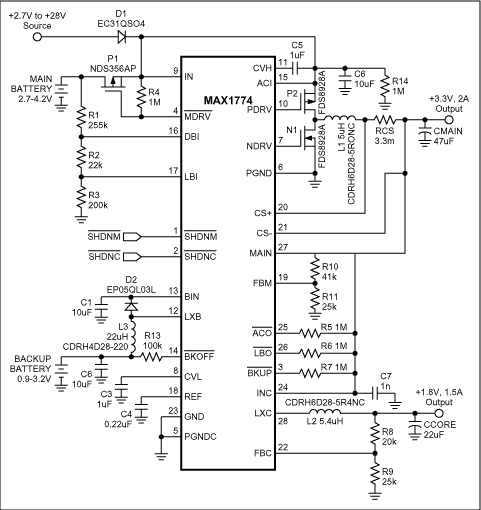
Figure 4. This fully integrated approach allows the widest range of input voltage, and includes both a main and a backup battery. Its dual output makes the IC extremely versatile.
Outlined above are four different circuit topologies for power-supply switchover, and each option provides a backup battery for portability and brownout protection. The first example implements power-supply switchover with only a MOSFET and diode, and the fourth is a fully integrated option that improves the overall time to market. Between these extremes are many circuit variations for achieving the same ends. These examples are intended as starting points, to be optimized for specific applications.
A similar version of this article appeared in the February 2003 issue of Portable Design magazine.
最新メディア 21