Optimizing the Electronic Load for High-Current, Low-Voltage Power Supplies, Part 1
Read other articles in this series.
要約
This first part of a three-part tutorial on high-performance electronic loads for testing high-current, low-voltage power supplies describes the need for special electronic loads, such as special electrical characteristics that are required. It also provides a comparison between "off-the-shelf" test equipment and specially designed load circuits. A similar version of this tutorial originally appeared on March 13, 2020, in Electronic Design.
Why Bench-Top Electronic Loads Fall Short
Electrical power requirements for modern CPUs, GPUs, FPGAs, and ASICs continue to increase, both in magnitude and in performance. Supply current requirements have risen to the hundreds of amperes, and power-supply bandwidth needs to be above 100kHz to meet stringent transient-response requirements. At the same time, supply voltages are trending downwards, with most core voltages now below 1V and some as low as 300mV. These trends make it increasingly difficult to characterize the performance of a suitable power supply using conventional “bench top” electronic loads.
Performance Limited By Resistive Losses and Parasitic Inductance
Commercially available electronic loads combine excellent precision with sophisticated control interfaces and can sink very high current at high power. The Chroma 63600 series provides a good example. Several different models are available in this series, each tailored to a different range of voltage, power, and current. The model with the lowest headroom requirement is the 63640-80-80, which can sink about 80A from a 400mV supply, as shown in Figure 1. This operating point reveals that its lowest achievable resistance is near 5mΩ. Each of these loads can sink up to 80A, limited to 400W.
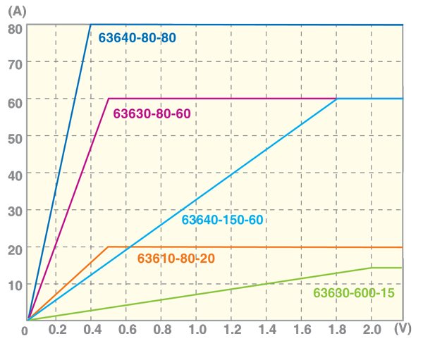
Figure 1. Chroma 63600 series voltage and current headroom characteristics. Image courtesy of Chroma USA.
This is impressive performance. But to test a 300A, 0.8V power supply, at least four 63640-80-80 load modules must be combined in parallel, both for an effective on-resistance below 2.7mΩ and to handle the total current. The Chroma 63600-5 Load Mainframe allows us to do exactly that, combining up to five load modules in a single chassis, with coordinated control and measurement functions.
However, despite their excellent specifications, the overall performance of an array of benchtop loads is fundamentally limited by their electrical connection to the supply under test. For example, Figure 2 shows how a high-current power supply might be connected to a bank of electronic loads for testing.
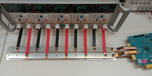
Figure 2. A parallel array of benchtop electronic loads with bus bar connections to an evaluation kit.
Copper and aluminum “bus bar” conductors are used to make the connection, with five electronic load modules operating in parallel to handle the current and power. Unfortunately, the form factor of this test setup requires high-current conductors to span 40cm or more, and this path length imposes significant resistive loss between the supply under test and the load modules. This added resistance cuts into the voltage headroom at the load, and parasitic inductance LP in the conductors sets an inescapable upper limit on the maximum load transient slew rate that can be achieved.
dI/dtMAX = VDUT/LP
Vexingly, the more individual loads that are combined in parallel, the larger the test setup becomes and, accordingly, more resistive and inductive losses are incurred in the connection bus. Clearly, a more specialized electronic load solution is needed to achieve the highest slew rate and lowest total resistance.
What’s Needed in an Electronic Load?
To emulate the behavior of the semiconductor device being powered, we need an electronic load with all the following characteristics:
- Load-current slew rate (dI/dt) as high as possible (ideally, the slew rate is also adjustable)
- Precisely adjustable load current
- High power dissipation capability, both peak and continuous
- Ability to monitor the load current with high fidelity and wide bandwidth
For testing low-voltage power supplies at very high current levels, the electronic load must have ultra-low minimum “on-resistance.” Finally, the electronic load must be designed to connect to the supply under test with minimal resistance and inductance, or the overall performance will be limited by the interconnect itself.
Electronic Load Options for Power Supply Testing
Simple Resistive Load
A power resistor provides one of the simplest loads. If sized and cooled correctly, it could satisfy the requirement for high power dissipation, and current can be monitored directly (by measuring the voltage across the known resistance.) Adding a switch in series makes it possible to generate a load transient – but the load will either be fully on, or completely off - and the current would be dependent upon the voltage under test. The current slew-rate is neither controlled nor adjustable. Clearly, this is not a flexible solution that can be adapted to a wide range of testing requirements.
Active Current-Sink Based on an Op Amp
To provide variable load and controllable current slew-rate (the rate at which the load current rises and falls), it is necessary to construct an active current-sink circuit based around an operational amplifier. The topology of this circuit is shown in Figure 3. An operational amplifier drives the gate of a power MOSFET to establish a controlled voltage across a sense resistor. This results in a controlled load current that flows from the drain to the source of the MOSFET and through the sense resistor to ground. The power MOSFET adds current gain but does not add voltage gain because it is operating as a common-drain amplifier, also known as a source-follower.
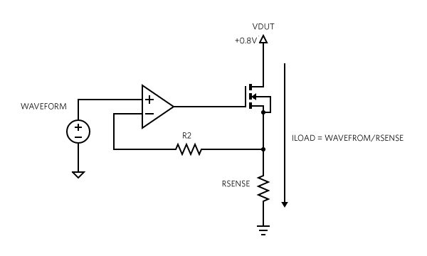
Figure 3. Basic active current-sink circuit.
This circuit can be implemented with an n-channel MOSFET with the sense-resistor on the low side, or with a p-channel MOSFET with the sense resistor on the high side. In the latter case, the circuit is more aptly described as a current source. Either way, the sense resistor adds a bit of negative feedback because it is connected at the source of the MOSFET, subtracting gate-to-source voltage as current increases and conversely adding gate drive as current decreases, which aids stability.
Figure 4 shows a practical implementation of an active current-sink circuit with an n-channel MOSFET. This circuit brings together the simple current-sink of Figure 3 with a differential amplifier. This topology improves precision by accounting for dynamic and static differences in ground potential between the input signal (SGND) and the low side of the sense resistor (GND).
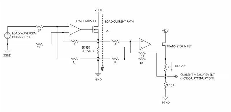
Figure 4. Detailed current-sink circuit.
The load current developed by this circuit is proportional to the voltage of a control signal (labeled Load Waveform in Figure 4), with gain set by the ratio of the input and gain-setting resistances. For example, using the principle of superposition to analyze the circuit of Figure 4, we see that the current follows the input signal, scaled by the gain of 1/2 and the sense resistance.
Load Current = (VS − GND)/RSENSE
VS = (Load Waveform) × (R/3R) × (1 + R/2R) – SGND × (R/2R) + GND × (2R/3R) × (1 + R/2R)
VS = (Load Waveform - SGND) × (R/2R) + GND
VS – GND = (Load Waveform – SGND) × (R/2R)
Load Current = (Load Waveform – SGND) × (1/2) / RSENSE
Thus, the sense resistor is referred to the power ground and the input signal is referred to the signal ground. The difference-amplifier configuration minimizes the detrimental effect of power-ground and signal-ground shift on the accuracy of the current sink.
The active current-sink circuit has many advantages compared to a simple switched resistance. Unlike a simple resistance, an active current sink can generate a variable load current from zero amps up to the maximum current. Further, because the load current is controlled by the operational amplifier in a closed-loop manner, the current tracks the control signal precisely, so the active current sink can achieve controlled current slew-rates. Finally, because there is a fixed-value resistive element in the circuit, precise high-bandwidth measurement of the load current is relatively simple. Figure 5 shows one way that a second amplifier can be added to report the load current; in this case, configured as a transconductance amplifier to allow easy summing of the current-measurement signals from multiple current-sink circuits.

Figure 5. Transconductance amplifier for current measurement.
Conclusion
With the fundamentals of the active electronic load circuit in hand, the next part of a successful design is component selection and circuit layout. Please watch for the second part of this three-part tutorial for more insights. Continue to read Part 2.
この記事に関して
製品
産業向けソリューション
製品カテゴリ
最新メディア 21