Op Amp Precision Positive & Negative Clipper using LT6015/LT6016/LT6017
Op Amp Precision Positive & Negative Clipper using LT6015/LT6016/LT6017
2016年10月03日
It can be a challenge to match the voltage range of an analog signal to the input range of an analog to digital converter (ADC). Exceeding the ADC’s input range will give an incorrect reading, and if the input goes far enough beyond the power supply rails substrate currents can flow into the ADC which can cause latch up or even damage to the part. However restricting the input voltage range to lower, more conservative levels wastes the ADC’s dynamic range and resolution.
The simple op amp clipper shown in Figure 1 prevents these problems. The maximum allowable input voltage is applied to the non inverting input of U1, and the output is fed back to the inverting input via small signal diode D1. The ADC’s reference voltage can be used for the clipping reference if it’s available. When the input voltage is below the reference, U1’s output is driven to the positive rail and D1 is reversed biased, so the input signal passes through without being altered. When the input goes above the clamp voltage, the op amp output reverses and closes the loop through D1, effectively becoming a unity gain follower to the clamp voltage. The input resistor R1 limits the amount of current the op amp output has to sink. The second op amp U2 performs the complementary negative clipping function, preventing the signal from going below ground. Thus the output signal is restricted to 4.096 V to 0 V out in this example.


Figure 1. LT6015 Precision Positive & Negative Clipper
While simple in concept, this circuit poses unique challenges for the op amp. First, most modern op amps have back to back diodes across the input to prevent the application of large differential voltages to the inputs which can cause damage to the part or shifts in the input offset voltage. In this circuit these diodes would prevent the output signal from going more than 1 diode drop below the positive clamp voltage or 1 diode drop above the negative clamp voltage. Deciding whether a given op amp has these diodes can require some detective work. Some parts’ data sheets show the presence of the input diodes, but others don’t. Another indication of the diodes’ presence is a limitation in the Absolute Maximum Ratings section of input current to a few mA.
In addition the output of the op amp has to slew from the “unclamped” to the “clamped” state as quickly as possible in order to clamp a fast rising signal without a potentially dangerous overshoot. Further, rail to rail input and output operation of the op amp is desired so it can function with voltages close to the limits of the power supplies.
The LT6015 family of op amps, which includes the LT6016 dual and LT6017 quad versions, address these issues. There are no diodes on the inputs so they are permitted to have a ±80 V differential voltage which should not impose a limitation on any practical ADC application. Further, the input voltage can go as high as 80V above or 25V below the –V rail, which allows the part to survive inputs that would damage other parts.
The LT6015 is further unique in that it allows a power supply range from V+ to –V of up to 60V, which would allow use of the circuit to clamp higher voltages than the great majority of op amps. It also has a slew rate of 0.75V/µs which allows it to clamp reasonably fast rising signals. The sub 100µV typical offset voltage ensures that the clamping level is very accurate.
Figure 2 shows the LT6105 driven from ±10 V supplies clamping a 7Vpk–pk, 1kHz sine wave at 0V and 4V. It’s hard to see the clamping action, but if you zoom in on the output you can see a small overshoot in Figure 3.


Figure 2. LT6105 Positive & Negative Clamping Action


Figure 3. LT6105 Small Overshoot On Clamping
Increasing the input frequency to 30kHz in Figure 4 clearly shows the clamping action taking place in less than 10µs, limiting the operating bandwidth of the circuit to a few kHz. The clamping speed can also be increased by limiting the voltage supply rails to close to the clamping limit voltages, which lowers the voltage range the output must slew to go into clamping mode. Since the LT6105 output swings very close to the supply rails, little extra voltage range is required.

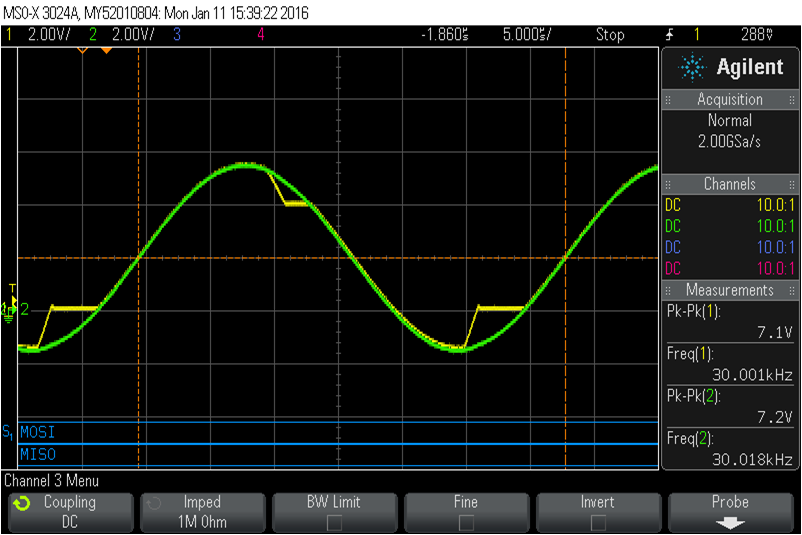
Figure 4. LT6105 Clamping Speed
Another limitation on this circuit is that the output resistance is defined by R1, which needs to be at least a few hundred ohms in order to limit the output of current in the op amp output. Some ADCs need to be driven by a low resistance so buffer amp U3 might be required. The LT6017 quad package would permit a single part to perform all these functions.
The LT6015 is offered in a 5-lead SOT package. The LT6016 dual op amp is available in an 8-lead MSOP package. The LT6017 is offered in a 22-pin leadless DFN package.
著者について
Thomas Mostellerは、アナログ・デバイセズのフィールド・アプリケーション・エンジニアです。1990年から米国中部大西洋岸地域を担当し、防衛、民生、産業などの分野でお客様に対する設計支援を行ってきました。主なアプリケーションとしては、配電/給電、アナログ・シグナル・コンディショニング、データ変換、RF/通信などが挙げられます。Linear Technology(現在はアナログ・デバイセズに統合)に入社する前は、10年間にわたって...
最新メディア 21