MAX38888 - Configuring the Backup Voltage Within 5% of the Minimum Charging Voltage
要約
This application note proposes a reference circuit design using the MAX38888. The MAX38888 provides a supercapacitor-based power backup in the absence of the system rail (VSYS) by discharging its stored charge. The backup voltage provided by the regulator from the super cap is 12.5% less than the system rail (VSYS) when the system rail (VSYS) is removed. The reference design in this application note explains how to maintain the backup voltage within 5% of the minimum SYS charge voltage. This application enhancement is for applications that require a backup regulation window tighter than 5% or less than the minimum charging voltage (VSYS).
Introduction
The demands for backup power applications are on an unabated rise as the demand for high performance portable electronic devices, IoT, metering devices, and handheld devices is growing. It often becomes essential to supply backup power efficiently and quickly with the indication of backup availability.
The MAX38888 is a super capacitor-based bidirectional power transfer regulator with a shared inductor used in power backup applications. The MAX38888 eliminates the need for an additional power converter while combining the buck and boost operations in a single IC with the least external component count, thus maximizing cost savings.
This application note discusses the MAX38888-based super capacitor backup regulator with programmable backup voltage, and how to keep the backup voltage within 5% of the minimum SYS charge voltage.
About the MAX38888 Reversible Buck/Boost Regulator
The MAX38888 reversible buck/boost regulator charges the storage capacitor when there is input voltage and provides a regulated system output during power interruption. The MAX38888 is a storage capacitor or capacitor bank backup regulator designed to efficiently transfer power between a storage element and a system supply rail in reversible buck and boost operations using the same inductor.
The regulator operates in the buck mode when the main supply is present and above the minimum charge supply voltage. It charges the storage element at up to 500mA peak inductor current (RISET-20K). Once the storage element is charged, the circuit draws only 2.5µA of current while it maintains the super capacitor or another storage element in its ready state. The regulator operates in the boost mode and prevents the system from dropping below the minimum operating voltage when the main supply is removed, discharging the storage element at up to 2.5A peak inductor current (RISET-20K).
| Features | Performance |
|
Figure 1. Charge and discharge waveforms. |
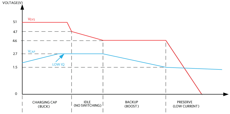
Figure 2 shows the typical application circuit of the MAX38888 buck/boost regulator.

Figure 2. Typical application circuit of the MAX38888.
Need for Tighter Regulation During the Backup Mode
Some applications work within ±5% of the supply voltage. Examples like RS232, RS-485, etc. require tighter regulation of the supply voltage while in the backup mode. The SYS voltage is derived from downstream regulators in a few applications. So, there is a need for tighter regulation during backup. The backup voltage of MAX38888 is 12.5% less than the minimum charging SYS voltage as of now. The MAX38888 backup voltage can be configured within 5% of the minimum charging SYS charge voltage with the proposed solution.
The following use case is considered here:
- Minimum SYS charge voltage = 5.1V
- Super cap voltage range = 1.5 V to 2.7V
- Peak inductor current in discharge mode = 2.5A.
- Peak inductor current in charge mode = 0.5A
- Backup voltage in absence of system voltage = 4.46V (without additional circuitry)
- Backup voltage in absence of system voltage = 4.85V (with additional circuitry)
Circuit Description
Figure 3 shows the circuit diagram with an additional circuit to regulate the backup voltage to be within 5% of the minimum SYS voltage.

Figure 3. Circuit diagram with reducing hysteresis.
The MAX9064 is a nanopower comparator with an integrated voltage reference of 200mV, which is rated to consume only 40nA (typ) operating current. The comparator is configured with trip points using voltage divider resistors Rf1 and Rf2 (Figure 3) from the SYS voltage to activate a pair of NMOS signal MOSFETs. The comparator trip voltage is set at 4.95V in this case. Two N-channel FETs Q1 and Q2 are used here, with low on-state resistance.
The MAX38888 enters the charge mode depending upon the FBS and FBCH voltages. It enters the charge mode of operation if the FBS voltage is greater than 0.56V and FBCH is less than 0.5V.
The voltage at the non-inverting terminal of the comparator is greater than the internal threshold voltage during the charge phase. Therefore, the output of the comparator goes high, driving the MOSFET Q1. Q1 turns ON and Q2 turns OFF.

The FBS voltage is set by the R6, R5, and R10 resistors as the Q2 is turned off. Here, 5.1 is the minimum system charge voltage.
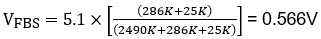
The VFBS ? 0.56V and VFBCH < 0.5V. So, the super capacitor charges up to 2.7V. The RDY flag asserts and the circuit draws only 2.5µA of current while maintaining the storage element in its ready state.
The minimum boost/backup voltage of the MAX38888 depends upon the resistor divider connected from the SYS to GND and VFBS voltage. The regulator boosts only when VFBS < 0.5V.
The comparator trip voltage is set at 4.95V when the SYS voltage is removed. Once the minimum charging SYS voltage is below 4.95V, the non-inverting terminal of the comparator is lesser than the internal reference voltage. Therefore, the output of the comparator goes low, driving the MOSFET Q1. Q1 turns OFF, which turns ON MOSFET Q2, thereby shorting the Resistor R10. So, the FBS Voltage is set by the R5 and R6 resistors only.

The MAX38888 boosts to the voltage is given by:
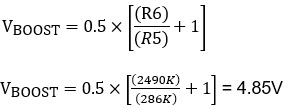
Now the backup voltage is 4.85V instead of 4.46V. Some applications where the ripple at the SYS pin is higher require higher capacitance at the SYS pin to avoid the back and forth between the charge and discharge operations.
Circuit Operation Waveforms - Before and After Modification

Hi-res Image ›
Figure 4. The difference in the circuit operation before and after modification
The MAX38888 boosts to 4.85V with additional circuitry during backup.

Figure 5. Comparing the difference in the backup voltage and showing the comparator threshold.
Results

Figure 6. Comparing the results.
Conclusion
The MAX38888 is a highly integrated, high-performance supercapacitor regulator, which can be implemented for backup in a wide range of applications. The above reference, schematic, and waveform captures can be used for a super cap-based backup regulator configuring the backup voltage within 5% of the minimum charging voltage with choice of resistors, MOSFET, and comparator. The proposed solution enables the applications that require tight regulation in backup.
{{modalTitle}}
{{modalDescription}}
{{dropdownTitle}}
- {{defaultSelectedText}} {{#each projectNames}}
- {{name}} {{/each}} {{#if newProjectText}}
-
 {{newProjectText}}
{{/if}}
{{newProjectText}}
{{/if}}
{{newProjectTitle}}
{{projectNameErrorText}}
最新メディア 21


