積層型負荷のアーキテクチャを改善する
はじめに
エレクトロニクスで使用される電源電圧は低下する傾向にあります。その一方で、負荷電流が増加し続けているアプリケーションも存在します。典型的な例としては、AIを活用するアプリケーションにおけるサーバの負荷電流が挙げられます。そのようなアプリケーションでは、プリント基板上で生じる伝導損失が問題になる可能性があります。実は、この問題の解決策になり得ると考えられている手法が存在します。それは、積層型のパワー素子と、電力差を処理する仕組みを組み合わせるというものです1~4。また、この手法が登場する前には、エネルギー交換器の概念に関する研究結果が発表されていました1。ただ、その研究は電力差の処理だけに注目したものでした。そのアーキテクチャにおいて、システムの電源レールに現れるのは平均電流であり、直列に接続された素子の最小電流ではありません。一般に、損失は処理に伴う電力に比例します。したがって、その電力を減らすことが損失の低減につながります。このことは、エネルギー交換器にも当てはまります。エネルギー交換器のアーキテクチャで使用できる回路の種類は1つに限られるわけではありません。異なるコンデンサ回路(スイッチト・キャパシタ回路)を含めて、異なる変換器を使用できることに注目すべきです1。
負荷過渡応答を積極的に管理する必要があるアプリケーションでは、上記の概念の改善が試みられつつあります。具体的には、高速な負荷変動に対処するための手段として電圧レギュレータ(以下、VR)を追加する方法が検討されています2、3。その結果、AIの市場を意識した低電圧/大電流のアプリケーションを対象とするプロトタイプのボードが開発されました4。そのボードでは、スイッチト・キャパシタ回路で実現されたシングルエンドのエネルギー交換器が使われていました3。ただ、予想されたとおり、シングルエンドのエネルギー交換器によって大きな電力差を処理すると、負荷(VOのレール)に影響を及ぼす多くのノイズが生成されることがわかっています。そのボードでは、250Wの全負荷の条件で約86%のシステム効率が得られると報告されています。また、バイアス回路を改良すれば、効率が約2%改善する見込みだと説明されています。
積層型負荷の概要
本稿では、450Wの全負荷時に95%を超える効率が得られる積層型負荷のプロトタイプを紹介します。また、上述したエネルギー交換器に関する重要な改善方法を示します。
図1に、積層型負荷のプロトタイプのブロック図を示しました。メインのVR(VR_total)は、できるだけ高い効率が得られるようにすることを主な目的としたものです。このVRは、フル・パワーで積層型負荷に対する給電を実施します。4つの高速VR(VR_1~VR_4)は、それぞれに対応する負荷に対する給電を担います。その出力は高い精度でレギュレートされており、それによって過渡応答が処理されます。負荷が理想的な状態でマッチしていれば、これらの高速VRは電力差に対応するための処理は行いません。負荷にミスマッチがある場合だけ、その電力差に依存した処理を実行することになります。負荷の差が最大になったとしても、その値は全負荷よりも小さいと考えられます。そのため、高速VRの熱設計は、メインのVRよりはるかに少ない電流を前提として行われています。一方で、高速VRの主機能の設計については、それぞれに対応する負荷のフルスケールの過渡的な変化に対応できるようにすることが重要です。すべての負荷が平均的に見ればかなりマッチしていたとしても、すべての過渡的な変化(ステップ)が完璧にマッチしているとは考えにくいでしょう。また、より低速なメインのVRは、出力電流の調整により長い時間を要します。

図1. 積層型負荷のプロトタイプ。そのブロック図を示しています。
エネルギー交換器の改善
エネルギー交換器は、高速VRの全入力レールの間で電力交換を実行します。メインのVRによって直列に接続された線形負荷だけを駆動する場合、出力電流は最も小さい負荷に依存します。それに対し、エネルギー交換器を追加すると、メインのVRの出力電流は、すべての負荷の平均電流という理想的な値になります。但し、実際には高速VRとエネルギー交換器の損失を補償するために、出力電流はそれよりも少し高い値になります。
図2に示したのはシングルエンドのエネルギー交換器を適用した例です。一方、図3には差動型(完全差動型)のエネルギー交換器を適用した例を示しました。この差動型のエネルギー交換器が本稿で提案する回路です。以下では、これら2つのエネルギー交換器について説明します。


図3. 差動型のエネルギー交換器(EE2)1
まず、図2に示したシングルエンドのエネルギー交換器に注目します。実は、この回路には1つ問題があります。それは、各フライング・キャパシタからのリターン電流が、直列に接続されている各負荷のバルク・キャパシタ(コンデンサ)COに流入/流出するというものです。それらの充放電電流には、降圧コンバータ(メインのVRと高速VRの両方)の出力電流と比べてはるかに高速なAC成分が含まれます。図4(a)に示したのは、シングルエンドのエネルギー交換器を採用したシステムのシミュレーション結果です。このシミュレーションでは、図1の負荷RL4に50Aのステップ状の電流を印加します。これを見ると、電流を印加する前から、すべてのレールに認識できるレベルのノイズが現れています。そして、電流が印加され、エネルギー交換器がVR_4の入力に電荷を移動させ始めると、ノイズが著しく増大しています。

図4. 積層型負荷のシミュレーション結果。負荷RL4に50Aのステップ状の電流が印加された場合の各種の信号波形を示しました。(a)は図2に示したシングルエンドのエネルギー交換器、(b)は図3に示した差動型のエネルギー交換器を使用した場合の結果です。
図4(b)に示したのは、差動型のエネルギー交換器を使用した場合のシミュレーション結果です。これを見ると、図4(a)に現れているノイズの問題が解消されていることがわかります。差動型のエネルギー交換器を使用した場合には、それが原因で負荷または負荷レールのCOに流れる電流が存在しないからです。
図5に示したのは、積層型負荷を採用したシステムのプロトタイプです。実際には、エネルギー交換器だけが異なる2つのバージョンを設計しました。1つ目のバージョンには、図2に示したシングルエンドのエネルギー交換器を実装しています。2つ目のバージョンには、図3に示した差動型のエネルギー交換器を実装しました。
これらのプロトタイプを使用して実測評価を行いました。高速に遷移する負荷は、プラガブル・モジュールを使用して実現しました(図5は、モジュールを1つだけ接続した状態を表しています)。そのようにしてシステムの動的性能の評価を実施しました。メインのボードは、高速VR用のコネクタも備えています。これを利用すれば、高速VRのモジュールを簡単に調整/変更することができます。

図5. 積層型負荷を採用したシステムのプロトタイプ
評価結果
図6に示したグラフをご覧ください。これは、負荷のバランスがとれた状態で動作するシステム全体(12Vの入力と制御回路に依存するすべてのバイアス回路を含みます)の効率を示したものです。この評価は、個々の負荷電圧が0.8V、0.9V、1.0Vの条件で実施しました。2種類のエネルギー交換器EE1、EE2のどちらを使用した場合も効率はほぼ同等です。VO = 4×0.9V = 3.6Vの公称動作条件の下で、全負荷時の効率は95%を超えています。すべての負荷を並列に配置した場合、VO = 0.9Vの単一のレールに500Aの電流が流れることに注意してください。95%を超えるシステム効率は、この条件における公表済みの効率の値を明らかに上回っています。その主な要因は2つあります。1つは、4つの負荷を直列に接続することにより、出力電流が1/4に低減されることです。もう1つは、メインのVRによってVSTACKの4倍(4×VO)のフル・パワーで給電が行われることです(一般にVOが高いほどVRの効率は高くなります)。

図6. エネルギー交換器を使用する場合のシステムの効率。シングルエンドのエネルギー交換器EE1と差動型のエネルギー交換器EE2を使用した場合の結果です。VOのレールの値が異なる3種類の条件で測定しました。
このプロトタイプのボードは、市販の部品を使用して構築しました。つまり、各コンポーネントの最適化は行っていません。それにもかかわらず高い効率が得られた理由の1つは、メインのVRのモジュールと高速VRのモジュールに使われている結合インダクタにあります。
一般に、結合インダクタを使用する場合、合理的なサイズのものを選択しつつ、スイッチング周波数を低く抑えることができます。その結果、スイッチング損失を削減することが可能になります。これは、高速VRにおいて特に重要なことです。負荷のバランスがとれている場合、高速VRが処理しなければならない電力は大きくありません。それでもスイッチング損失はできるだけ少なく抑えるべきです。
図7、図8は、VO1のレールとVR1の入力電源レールの電圧リップルを示したものです。図7はシングルエンドのエネルギー交換器、図8は差動型のエネルギー交換器を使用した場合の結果です。図7、図8の各波形は同じ条件下で取得しました。しかし、2つの図を比較すると大きな違いがあることがわかります。この例では、VO4のレールの負荷電流IOは50Aで、その他のレールの電流はゼロです。したがって、エネルギー交換器は他のレールからVO4のレールに多くの電力を移動させることになります。シングルエンドのエネルギー交換器は、COの寄生容量を介してVO1のレールに大きなスパイクを生じさせます4。それに対し、差動型のエネルギー交換器は、VOのレールには影響を与えません。(スイッチト・キャパシタ回路ではなく)降圧コンバータの電流に関連したはるかに短い時間スケールの小さなリップルが生じるだけです。
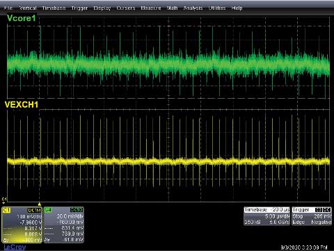
図7. シングルエンドのエネルギー交換器(図2)を使用するシステムの電圧リップル。VO1の電圧リップル(>60mV)とフローティング状態のVIN1の電圧リップル(>300mV)を示しています。
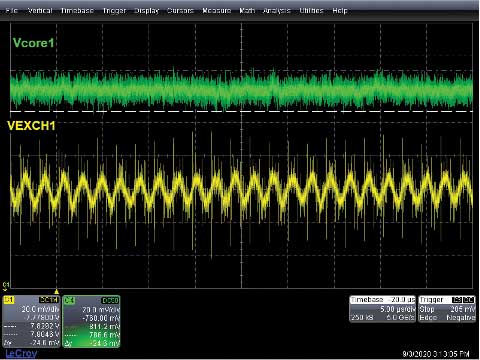
図8. 差動型のエネルギー交換器(図3)を使用するシステムの電圧リップル。VO1の電圧リップル(約25mV)とフローティング状態のVIN1の電圧リップル(約70mV)を示しています。
シングルエンドのエネルギー交換器を使用する場合、60mV(0.9VのVOの6.6%)を超える高速な電圧スパイクが生じます。それに対し、差動型のエネルギー交換器を使用した場合には、同スパイクを25mV(0.9VのVOの2.8%)未満に抑えられます。これが最も重要な効果です。差動型のエネルギー交換器の場合、電圧リップルに高周波のスパイクは全く含まれておらず、降圧コンバータのリップル電流に伴うリップルだけが現れます。この結果は、シミュレーション結果から予想される傾向と一致しています。電源レールの高速なスパイクは、デジタル回路に悪影響を及ぼす可能性があります。したがって、この問題はぜひ緩和すべきです。今後、VOの値は更に低くなると予想されます。そのため、ノイズの振幅が同じままでも、負荷の高速な動作に及ぶ影響は増大します。
図3に示した差動型のエネルギー交換器には、ノイズを改善するためのもう1つの方策が適用されています。それは、個々のフライング・キャパシタに対応するスイッチング動作の位相をずらすというものです。図2に示したシングルエンドのエネルギー交換器では、すべてのキャパシタを同時にスイッチングする必要があります。そのため、位相をずらすという対策は不可能です。この点は注目に値します。
図9は、差動型のエネルギー交換器を使用した場合の高速な負荷過渡応答を示したものです。図9(a)は、VO1のレールに100Aのステップ状の負荷電流が印加された場合の結果です。一方、図9(b)は100Aのステップ状の負荷電流を停止したときの波形を表しています。他のレールには負荷は接続されていません。そのため、最初は高速VR1が100Aの電流のすべてを供給します。メインのVRから25Aの平均電流が供給されたら、高速VR1は75Aだけを負荷に供給するようになります。VO1のレールのドループの変化を見ると、メインのVRが25Aの平均電流を供給するまでに要する時間は約10マイクロ秒です。それに伴って高速VR1のドループが減少することがわかります。そうすると、VR2、VR3、VR4の各レールの電流は25A少なくなり、その電力がエネルギー交換器とVR1に移動します。ここで、エネルギー交換器の電圧はレギュレートされていません。したがって、高速VR1の入力レールがセトリングするまでには、10マイクロ秒以上の時間がかかります(黄色のトレース)。

図9. 負荷過渡応答の例。(a)はVO1のレールに100Aの負荷電流が高速に印加されたときの波形です。(b)は負荷電流を停止したときの波形です。
まとめ
本稿では、積層型負荷のプロトタイプについて説明しました。そのプロトタイプは、想定していた完全な機能を実現しています。その評価結果から、VOとトータルのPOの条件が同じである場合、従来のアーキテクチャを使用するよりも、本稿で提案したアーキテクチャを使用した方が全般的に高い効率が得られることが明らかになりました(VOが0.9V、POが450Wの条件で、95%を超える効率を達成)。このプロトタイプのボードは、市販のコンポーネントを使用して構成したものです。お客様の仕様に合わせて最適化を施せば、更に高い性能が得られる可能性があります。
積層型負荷に給電するという概念は、効率の改善という観点からは非常に有望な手法だと言えます。配電に伴う損失が大幅に減少し、負荷電圧VSTACKが高いほどメインのVRがより高い効率で動作するからです。負荷を高い密度で配置すれば、負荷電流の大幅な減少によってプリント基板における損失の改善効果は更に大きくなるはずです。この点も注目に値します。実際のアプリケーションでは、大電流/低電圧に対応する負荷が非常に高い密度で配置される可能性があります。そのため、配電に伴う損失がより大きな課題になるでしょう。そのようなアプリケーションで積層型負荷を採用すれば、プロトタイプのボードで得られた結果を上回る大きな改善効果が期待できます。
本稿では、エネルギー交換器に関する既存のコンセプト1を基に、フローティング状態のレールを対象として差動型のエネルギー交換器を使用する方法を提案しました。その手法を採用すれば、あらゆる負荷条件の下で、すべての高速電流とそれに伴う電圧スパイクを排除できます。そのため、負荷の電圧レールにおけるノイズ性能が大幅に改善されます。
参考資料
1 Anthony J. Stratakos、Alexandr Ikiannikov「System, Method, Module, and Energy Exchanger for Optimizing Output of Series-Connected Photovoltaic and Electrochemical Devices(直列接続した太陽光発電デバイスと電気化学デバイスの出力を最適化するためのシステム、手法、モジュール、エネルギー交換器)」U.S. Patent 9,331,499、2011年4月
2 Enver Candan、Pradeep S. Shenoy、Robert C. N. Pilawa-Podgurski「A Series Stacked Power Delivery Architecture with Isolated Differential Power Conversion for Data Centers(絶縁型差動電力変換機能を備える直列積層型のデータ・センター用給電アーキテクチャ)」IEEE Transactions on Power Electronics、Vol. 31、No. 5、2016年5月
3 Shuai Jiang、Gregory Sizikov、Mikhail Popovich「Power Balancer for Series-Connected Load Zones of an Integrated Circuit(ICの直列接続負荷ゾーン向けのパワー・バランサ)」U.S. Patent 10,985,652、2020年3月
4 K. Kshirsagar、D. Clavette、P. Kasturi、W. Huang「Power Loss Reduction in Power Distribution Network Through Vertical Stacking(垂直積層によって配電網の電力損失を低減する)」IEEE、2021年6月
*英語版技術記事はこちらよりご覧いただけます。
著者について
この記事に関して
最新メディア 21