要約
This application note describes the MAX5072 DC-DC converter, specifically designed to address the power-management needs of the ADSL2+ modem. It also provides a design guide for buck, boost, or buck-boost converters, and includes proven circuit schematics with major component-part numbers. It also briefly describes the ADSL2 and ADSL2+ standards.
The ADSL standard has evolved from ADSL, ADSL2, ADSL2+, and the "Extended Reach ADSL2" in the past few years, extending the data rates to 24Mbps on phone lines as long as 22,000 feet. While the ADSL2 standard specifies a downstream frequency band up to 1.1MHz, ADSL2+ specifies up to 2.2MHz, resulting in a significant increase in data rates on shorter phone lines. Figure 1 and Figure 2 show bandwidth, data-rate and distance covered using the different standards. ADSL2+ can also be used to reduce crosstalk when multiple ADSL services are present in the same binder.
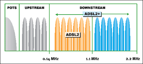
Figure 1. ADSL2 and ADSL2+ bandwidths used to carry data.
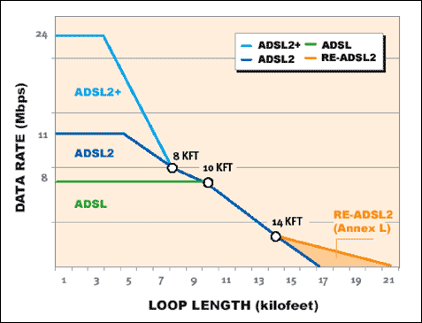
Figure 2. Data-rate and distance performance of ADSL, ADSL2 and ADSL2+.
As shown in Figure 1, the upstream direction uses from 25kHz to 138kHz and the downstream direction uses from 138kHz to 2.2MHz. This spectrum is divided into the carrier bands and each band is assigned a number of bits. The number of bits per carrier band depends on the signal-to-noise ratio (SNR).
The power-supply switching frequency significantly affects the noise floor, thereby reducing the overall bit rate. In the case of ADSL2+ where the downstream frequency band stretches up to 2.2MHz, we need to keep all the power-supply switching frequencies and their harmonics outside the 138kHz to 2.2MHz band. The ripple amplitude and its frequency equally impact the number of bits per carrier band. The 2.2MHz power-supply switching frequency has two advantages. First, it keeps the fundamental and its harmonics above the ADSL2+ spectrum. Second, the higher switching frequency reduces the peak-to-peak output ripple, even when using low-cost ceramic or aluminum electrolyte capacitors.
MAX5072 Power-Management Solution for ADSL2+
The MAX5072 is specifically designed to supply power to ADSL2+ modems. The goal is to provide a compact, low-cost converter that operates beyond the ADSL2+ frequency band and can be powered by an inexpensive AC adapter. It is a dual-output DC-DC converter with integrated high-side n-channel power MOSFETs, with each converter capable of operating up to 2.2MHz.
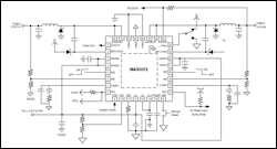
Figure 3. The MAX5072 dual-output buck converter offers switching-frequency operation above the ADSL2+ band. The 2.2MHz individual converter's switching frequency and high integration provides lowest cost solution and highest bandwidth for multiple DSL types (ADSL/VDSL).
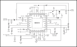
Figure 4. The MAX5072 dual-output buck and boost converter offers output voltage that is in the middle of the input-voltage range. The Buck Converter-1 output powers the Converter-2 (boost). The 3.3V powers the chipset and the 12V powers the line driver.
The output ripple frequency of the individual converters is 2.2MHz, however, the 180° out-of-phase operation of the individual converters doubles the input-capacitor ripple current frequency. This reduces the capacitor RMS current and size. Figure 5 and Figure 6 depict the switching waveforms of the dual-output DC-DC converters.
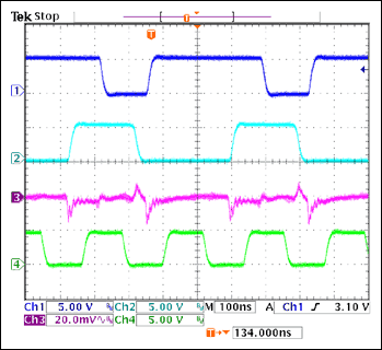
Figure 5. Dual buck-converter switching waveforms—input ripple. The individual-converter switching frequency is 2.2MHz, while the input-capacitor ripple frequency is 4.4MHz.
CH1 = SOURCE2, CH2 = SOURCE1, CH3 = input-capacitor ripple, CH4 = CLKOUT.
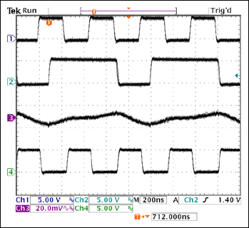
Figure 6. Dual buck-converter switching waveforms—output ripple. The output-capacitor ripple frequency is 2.2MHz, equal to the converter switching frequency. CH1 = SYNC, CH2 = SOURCE1, CH3 = Output1 Ripple, CH4 = CLKOUT.
Input/Output Voltages
The input voltage range of the MAX5072 is 4.5V to 5.5V or 5.5V to 23V. The voltages needed to power up the ADSL chipset include 1.2V, 1.8V, 2.5V, and 3.3V, in addition to the line-driver voltages of 5V or 12V. Both converters of the MAX5072 can be configured either as a buck converter or a boost converter. This makes various combination of voltage conversion possible with the MAX5072. Use Table 1 for the proper selection of a power-management scheme.
| Configuration | Input-Voltage Range (V) | Converter-1 (VOUT1 /IOUT1) |
Converter-2 (VOUT2 /IOUT2) |
| Dual buck | 4.5 to 5.5 (5V system input) | 1.2V/1.8V/2.5V/3.3V up to 2A | 3.3V up to 1A |
| 5.5 to 7 with transients up to 23V (6V AC adapter) | 1.2V/1.8V/2.5V/3.3V up to 2A | 3.3V up to 1A | |
| 7 to 12 with transients up to 23V (9V AC adapter) | 2.5V/3.3V up to 1.5A | 1.2V up to 1A (VOUT1 feeds Converter-2) | |
| 7 to 12 with Transients Up to 23V (9V AC adapter) | 2.5V/3.3V up to 2A | 5V up to 1A | |
| 11 to 16 | 3.3V up to 1.4A | 1.2V up to 1A (VOUT1 feeds Converter-2) | |
| 11 to 16 | 3.3V up to 1A | 5V up to 0.4A (VOUT1 Feeds Converter-2) | |
| Buck-boost (Converter-1 buck, Converter-2 boost) |
4.5 to 5.5 (5V system input) | 3.3V up to 1A | 5V up to 0.4A (VOUT1 Feeds Converter-2) |
| 4.5 to 5.5 (5V system input) | 3.3V up to 1A | 12V up to 0.4A (12V line driver) | |
| 7 to 12 with transients Up to 23V (9V AC adapter) | 3.3V up to 1A | 12V up to 0.2A (VOUT1 feeds Converter-2) | |
| 11 to 16 | 3.3V up to 1A | 12 up to 0.2A (VOUT1 feeds Converter-2) |
The large input-to-output voltage differential requires very-low-duty-cycle operation. The low duty cycle at 2.2MHz means low minimum controllable on time. The MAX5072 has a minimum controllable on time (tON-MIN) of about 100ns. Use the following equations to calculate the maximum allowable input voltage (VIN-MAX) for a required output voltage, without skipping the pulses.
Where VD is the forward-voltage drop of the Schottky rectifier (0.35V, typ), fSW is switching frequency of the converter, and tON-MIN is 100ns.
Similarly, the maximum duty cycle limit (DMAX) affects the minimum allowable input voltage for a required output voltage. Use the following equations to calculate the minimum input voltage (VIN-MIN) of the buck converter needed for a required output voltage VOUT.
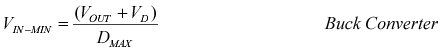
Where DMAX is at least 84% and VD is 0.35V.
The minimum input voltage allowable for the boost converter depends on the output voltage, peak current, and the inductor value.
To alleviate the minimum on-time issue or to limit switching losses, the switching frequency can be reduced. However, it is not possible to have different frequencies for two converters operating out of phase. Also, frequency beating can occur if the individual converter frequencies are not selected carefully. To avoid the minimum on-time and power-dissipation issues, the MAX5072 provides a frequency-select (FSEL1) pin. Connecting FSEL1 to ground reduces the switching frequency of Converter-1 to one-half the switching frequency of Converter-2 and one-quarter the internal-oscillator switching frequency. In this case, Converter-1 would be switching at 1.1MHz with Converter-2 switching at 2.2MHz. The input-capacitor ripple frequency would be 1.5 times the Converter-2 switching frequency and would have an asymmetrical ripple waveform.
MAX5072 Functions Needed for Multiple DSL Chipsets
- Power on reset (active-low RESET)— active-low RST is an open-drain output that pulls low when either output falls below 92.5% of its nominal regulation voltage. Once both outputs exceed 92.5% of their nominal regulated voltages and both soft-start cycles are completed, active-low RST enters a high-impedance state after the 180ms active time-out period.
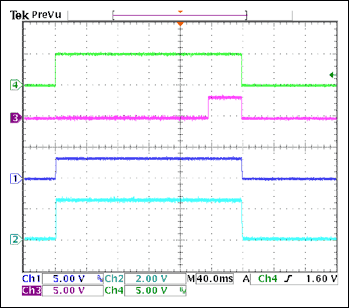
Figure 7. RESET active timeout period. The reset timeout period is internally fixed to 140ms. The RESET goes high 140ms after both outputs reach within regulation.
CH1 = VOUT1, CH2 = VOUT2, CH3 = RESET, CH4 = Enable. - Dying gasp (PFI/PFO)—Before powering down the modems, it is necessary to wrap up critical functions. The time needed to complete these functions is called the hold-up time. The input capacitors hold charge and provide energy to the converter after VIN is disconnected. The hold-up time (tHOLD) is defined as the time when the input voltage drops below VTRIP and the output falls out of regulation at the low end of the input-voltage range (VINMIN). Use the following equations to calculate the resistor divider and CIN required for proper hold-up time.
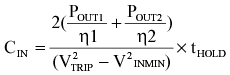
Where η1 and η2 (80% each, typ) are efficiencies of Converter-1 and Converter-2, respectively. - Manual RESET (active-low MR)—Microprocessor-based products require manual reset capability, allowing the operator or external logic circuitry to initiate a reset. A logic low on active-low MR asserts the reset. Reset remains asserted while active-low MR is low, and for the reset active time-out period (tRP) after active-low MR returns high.
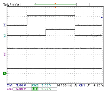
Figure 8. Manual RESET (active-low MR). The active-low MR includes internal debounce circuitry and saves the external active-low MR device. CH1 = active-low MR, CH2 = RESET, CH3 = VOUT1, CH4 = VOUT2
The following are some circuits designed for different xDSL modems.
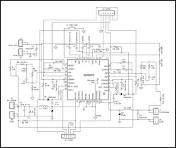
Figure 9. xDSL power-management solution. Input: 9V to 12V. Output: VOUT1 = 5V/550mA (up to 1A), VOUT2 = 1.2V/550mA (Up to 1A). The output-2 converter is powered from output-1. The switching frequency of each converter is 2.2MHz.
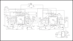
Figure 10. Multiple DSL (VDSL/ADSL) power management. Input: 5.5V to 7V, outputs: VOUT1 = 1.2V/1.5A, VOUT2 = 1.8V/1A, VOUT3 = 3.3V/1A, VOUT4 = 12.8V/200mA. The switching frequency of individual converter is 2.2MHz with a combined switching frequency equal to 8.8MHz. The switching frequency is synchronized to the system clock.
The complexity of high-frequency switching-converter design requires expertise and a great deal of design effort. However, the high-frequency switching payback is improved bandwidth. The designs provided are bench tested and can be used as is or as a starting point for new designs.
この記事に関して
{{modalTitle}}
{{modalDescription}}
{{dropdownTitle}}
- {{defaultSelectedText}} {{#each projectNames}}
- {{name}} {{/each}} {{#if newProjectText}}
-
 {{newProjectText}}
{{/if}}
{{newProjectText}}
{{/if}}
{{newProjectTitle}}
{{projectNameErrorText}}
最新メディア 20


