To meet the increasing demands for non-isolated Power over Ethernet (PoE) power solutions, Maxim has developed innovative, non-isolated PoE powered device (PD) power solutions. Each design was tested for load and line regulation, as well as efficiency and transient performance. As with all Maxim reference designs, the BOM, schematics, layout files, and Gerber files are all available and may be downloaded from the Design Resources tab. In addition, boards are available for purchase. These boards feature a module architecture, with through-hole pins for immediate board placement and accelerated prototyping.
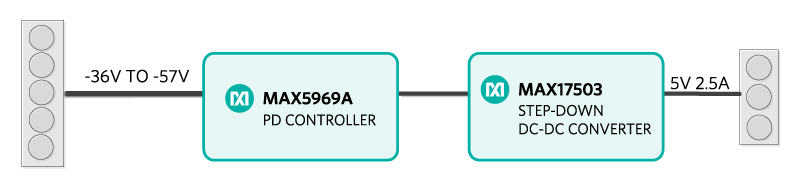
MAXREFDES98 combines the PD controller and the step down converter on a 14.0mm (0.55in) x 55.9mm (2.2in) board. The module accepts input voltages ranging from 36V to 57V, and provides an output voltage of 5V with current capacity of 2.5A.
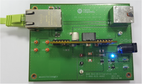
For initial evaluation, Maxim also provides an evaluation board, MAXREFDES98EV. This board features RJ45 connectors for quick testing with sourced power.
Power over Ethernet (PoE) provides power to Ethernet connected devices, through Ethernet lines, eliminating the need for connecting AC mains to the target devices. In addition to reducing cabling, PoE provides multiple advantages for many applications such as LED lighting, cameras, sensors, and additional equipment. These advantages include network management of devices, power measurement, and elimination of AC/DC circuitry.
Many PoE applications are isolated, to protect both people and systems from voltage and current transients. However, many applications do not require isolation, such as LED lighting and other equipment that is generally out of range for human touch. In these cases, eliminating the isolation circuitry further reduces cost and power dissipation at the PoE point of load. MAXREFDES98 is a unique PoE module reference design, providing 5V at 2.5A (12.5W) from a 36V to 57V input. This design can be used for evaluation, design, prototyping, and production.
MAXREFDES98 includes two function blocks: the PD controller block and the step down DC-DC power supply block. The PD controller uses the MAX5969A. The MAX5969A is an IEEE® 802.3af compliant, powered device interface controller with an integrated power MOSFET. The DC-DC power supply uses the MAX17503. The MAX17503 is a 4.5V~60V input, 2.5A output, high-efficiency synchronous step down converter with internal compensation. The entire design delivers a peak efficiency of 86% with an input of 48V.
The MAXREFDES98 features 12 through-hole pins spaced at a 2.54mm pitch standard. This modular architecture allows MAXREFDES98# to be soldered into a PCB or inserted into the MAXREFDES98EV for evaluation.
The MAXREFDES98 reference design contains all the control circuitry and electric components required for designing a 36V to 57V wide-input, 5V/2.5A (12.5W) output non-isolated step down converter power supply.
On the board, there are two 6-pin connectors. Table 1 and Table 2 provide the function of each pin.
Table 1
Pin #
Name
Function
1
VA1
Rectifier B Input Terminal 1
2
VA2
Rectifier A Input Terminal 2
3
VB1
Rectifier B Input Terminal 1
4
VB2
PD Classification Resistor Terminal 1
5
VB2
Rectifier B Input Terminal 2
6
CP2
PD Classification Resistor Terminal 2
Table 2
Pin #
Name
Function
1
VOUT
5V Output
2
VOUT
5V Output
2
VOUT
5V Output
3
VGND
Ground
4
GND
Not Connected
6
RESET
Reset Signal, Active Low
The MAXREFDES98 circuit consists of two function blocks: the PD controller and the step down DC-DC converter.
The PD controller section employs the MAX5969A. The MAX5969A provides a complete interface for a powered device (PD), compliant with the IEEE® 802.3af standard. The MAX5969A provides the PD with a detection signature, classification signature, and an integrated isolation power switch with inrush current control. Visit the MAX5969A product folder for more information.
When the MAXREFDES98 board is connected to PoE power sourcing equipment (PSE), the MAX5969A conducts the detection and classification process according to the IEEE 802.af/at standard. The on board classification resistor R1 (619Ω) sets the power rating to class 3, a maximum of 12.95W. On the MAXREFDES98EV board, there is one resistor place holder that can be used to change the power class. Refer to below table to select the appropriate R3 value on the MAXREFDES98EV# board.
Table 3. R3 value used to set PD classification class
Table 3. R3 Value Used to Set PD Classification Class
PD Class
Maximum Power Consumed by PD
R3 Value
Classification Current
IEEE 802.3 af/at Required Classification Current
Class 0
0.4W to 12.95W
Open
1.99mA
0mA to 5mA
Class 1
0.4W to 3.94W
143Ω
10.8mA
8mA to 13mA
Class 2
3.94W to 6.49W
75Ω
18.7mA
16mA to 21mA
Class 3
6.49W to 12.95W
47Ω
28.6mA
25mA to 31mA
MAX5969A provides one Power Good (PG) signal. Only after the MAX5969 internal hot-swap MOSFET switch is fully turned on, does the PG signal become active. PG is used as the signal to enable the DC-DC converter circuit. This process reduces the inrush current and the heat generated by the MAX5969 during startup.
The MAXREFDES98 reference design uses two bridge rectifiers, which make the design compatible with most PSE types. The bridge rectifiers cause power loss since there are always two diodes conducting, at the same time when the circuit is working. To improve efficiency, MAXREFDES98 uses low forward voltage Schottky bridge rectifiers. Test data shows that by using 100V/1A Schottky rectifiers (KMB110F), peak efficiency can be improved by about 1% compared to a traditional bridge rectifier such as the HD01-T.
Following the PD controller is the step down DC-DC converter. This circuit employs the MAX17503, Maxim's high efficiency, synchronous step-down DC-DC converter with internal compensation. For more specific information about the MAX17503, refer to the MAX17503 product folder. The MAX17503 circuit has been optimized for efficiency and reduction of inrush current using two different inductors. The system performs at a peak efficiency of 86% with a switching frequency to 300kHz, set with the RT resistor to 68kΩ.
For the inductor, MAXREFDES98 has been tested with the SLF12575T-150M4R7-PF from TDK and the HR320102-150 from HanRun. Test data shows these two inductors get nearly the same performance. In case you need to build your own circuit based on the MAXREFDES98# reference board, make sure the saturation current rating (ISAT) of the inductor is high enough so that saturation can occur only above the peak current-limit value of 3.7A.
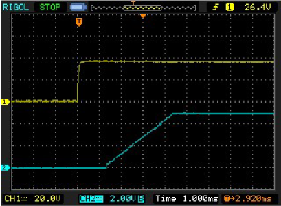
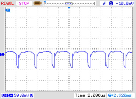
The MAXREFDES98 is set to a soft-start time to 3.2ms. A soft-start reduces the inrush current from the PSE. Figure 3 shows the soft-start waveform. The yellow trace is the enable signal (PG) from the MAX5969A, and the blue trace is the output voltage from the MAX17503.
Figure 3. Soft-start feature
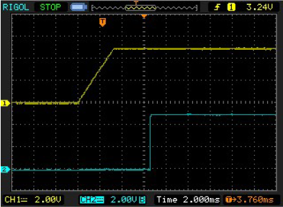
MAXREFDES98 reserves one RESET output pin (Pin 6 of J2, as described in table 2), which can be connected to the RESET pin of a microcontroller. This pin is open drain output, so users can OR (negative logic) it with another open drain signal, such as a watch dog circuit reset output, or manual reset switch. During the soft start phase, the RESET pin stays low. It goes high 3.4ms after the output voltage exceeds 4.75V. The blue trace in Figure 4 is the RESET signal, captured with an external 10kΩ resistor pulled up to VOUT. The yellow trace is the output voltage trace.
Figure 4. RESET goes high 3.4ms after VOUT exceeds 4.75V
RJ45 cable and one PSE RJ45 socket capable of delivering PoE, or one DC power supply adjustable to 57V
One electronic load
One voltmeter
Procedure
The MAXREFDES98 board is fully assembled and tested. Use the following steps to verify board operation.
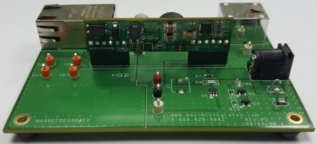
Insert the MAXREFDES98 board into the MAXREFDES98EV board, as shown in Figure 5.
Figure 5. MAXREFDES98# connected to the MAXREFDES98EV
Insert one end of the RJ45 cable to the PSE RJ45 socket, then insert the other end to J1 on MAXREFDES98EV# board, as shown in Figure 6. The "PWR" LED on right bottom corner should light up continuously or flash slowly, depending on the PSE.
In case the "PWM" LED does not light up, the RJ45 socket likely does not have the POE feature. In this case, connect the power supply (37V~57V) to VA1/VA2, or VB1/VB2. There is no polarity requirement when the power is connected, since there are bridge rectifiers following these connectors. When the power supply is turned on, the "PWM" LED should light up continuously.
Figure 6. When the MAXREFDES98 board works, the PWR LED on the MAXREFDES98EV board lights up
Connect the VOUT and PGND terminals on the MAXREFDES98 board to the electronic load.
Set the electronic load to a constant current up to 2.5A.
Connect the voltmeter to the VDC and GND, to verify the output voltage reading is 5V ±0.15V.
Set the electronic load to "short," and turn off the PWR LED. When the "short" is released, the PWR led should light up again, and the voltage should read 5V ±0.15V.
On the MAXREFDES98EV board, a current sense amplifier, MAX9643, measures the output current of the MAXREFDES98# board, and similar boards, such as the MAXREFDES108. To get the actual current, divide the voltage measured by 1.6. For example, if IOUT is measured at 1.6V, the actual current drawn from MAXREFDES98 board is 1A. The IOUT is designed to measure steady state current. If it is used to capture the transient current waveform, there will be distortion on the waveform due to MAX9643's signal bandwidth and pulse response. For more information, refer to the MAX9643 data sheet. Figure 7 shows the error curve of the current measurement circuit. Error increases as measured current decreases, as is consistent with any current measuring system.
The MAXREFDES98 design was verified and tested under the full input range and different output load conditions.
Power efficiency vs. load current
MAXREFDES98 performs with high efficiency, across a range of input voltages. Peak efficiency is 86%, and efficiency is high across a wide output current range.
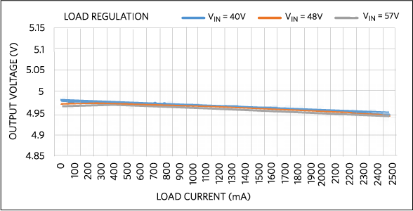
Figure 9. Load regulation
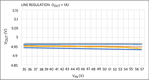
Figure 10. Line regulation when output current is 1A
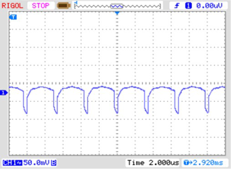
Figure 11. Output ripple at 5mA load
Figure 12. Output ripple at full load (2500mA)
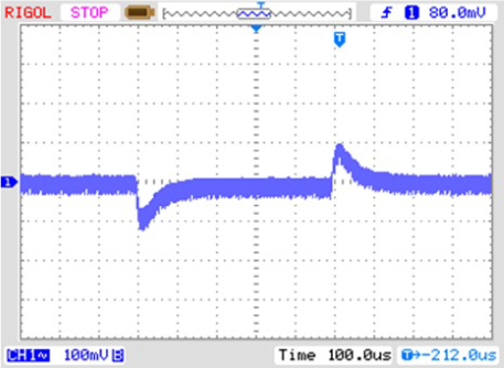
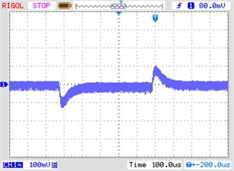
Figure 13. Load transient response when load steps between 5mA and 1000mA
Figure 14. Load transient response when load steps between 1500mA and 2500mA
IEEE is a registered service mark of the Institute of Electrical and Electronics Engineers, Inc.
Search our knowledge base for answers to your technical questions. Our dedicated team of Applications Engineers are also available to answer your technical questions.