MAXREFDES176


Overview
設計リソース
デバイス・ドライバ
コンポーネントのデジタル・インターフェースとを介して通信するために使用されるCコードやFPGAコードなどのソフトウェアです。
説明
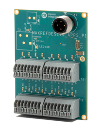
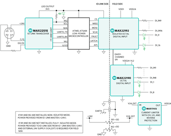
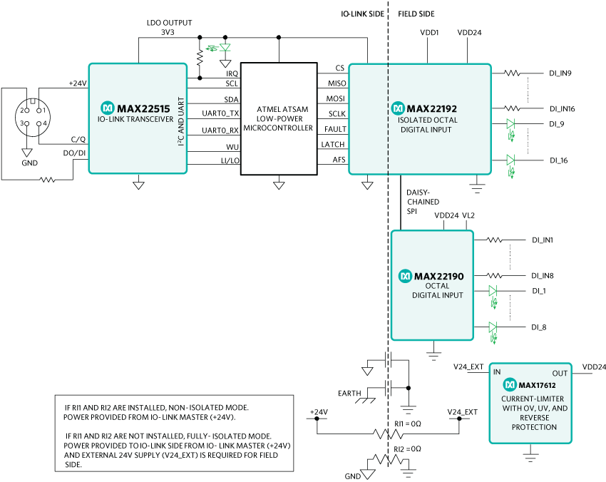
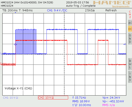
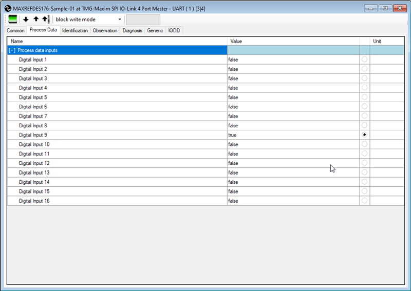
The MAXREFDES176# is a complete, IO-Link® 16-channel digital input hub reference design that consists of a MAX22515 IO-Link transceiver with integrated protection. It demonstrates an isolated digital input hub using the MAX22192 isolated octal digital input device daisy-chained with the MAX22190 octal digital input device to provide a total of 16 digital input channels.
Type 1 and Type 3 sensors are supported by default. Type 2 sensors can also be supported by modifying the resistor value that controls the value of the current sink within the devices. Built in an industrial form factor, the MAXREFDES176# uses an industry-standard M12 connector, allowing a 4-wire cable to be used. The digital input channels use industry-standard PCB terminal blocks.
In this design, an Atmel® ATSAM low-power microcontroller interfaces between the MAX22192 isolated digital input serializer and the MAX22515 IO-Link device transceiver. The MAX22515 features integrated surge protection for robust communication in a very small PCB area without requiring external protection components, such as TVS diodes. The MAX22515 is available in a tiny 20-bump WLP package, allowing the MAXREFDES176# to have a small footprint, though this is mostly determined by the size of the connectors. The design is reverse-polarity protected using the integrated active reverse-polarity protection of the MAX22515. The MAX22515 has two integrated LDO regulators (3.3V and 5.0V). The 3.3V LDO is used to generate the 3.3V supply for other circuitry, reducing the number of required external components and further saving space. The MAX22515 also features low on-resistance drivers (C/Q and DO/DI) to reduce power dissipation, allowing this reference design to consume minimal power with very low thermal dissipation.
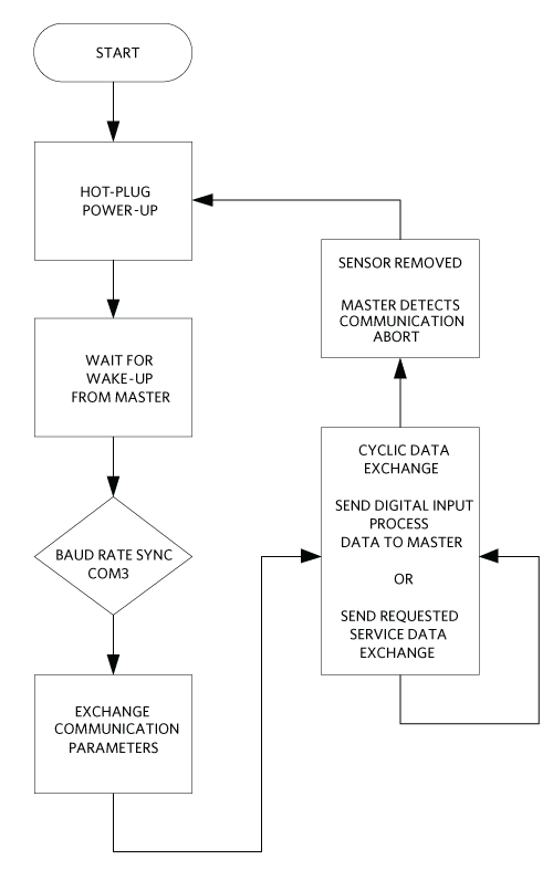
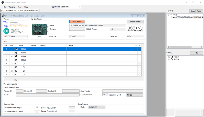
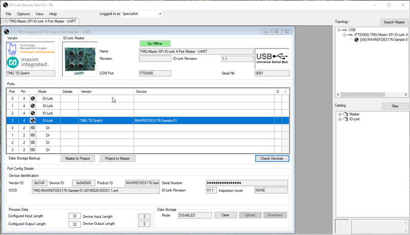
This IO-Link device utilizes the Technologie Management Gruppe Technologie und Engineering (TMG TE) IO-Link device stack to communicate to any IO-Link version 1.1-compliant master. The board contains a male M12 connector for connecting to a compliant IO-Link master using a standard M12 cable. Connecting the MAXREFDES176# to a USB IO-link master, such as the MAXREFDES165#, with the associated software allows for easy evaluation.
Design files, firmware, and software are available on the Design Resources tab. The board is also available for purchase.
機能と利点
- IEC 61131-9 Compliant
- TMG TE IO-Link Stack
- IO-Link Version 1.1 Compliant
- Integrated Galvanic Isolation
- On-Chip Serialization
使用されている製品
Details Section
Documentation & Resources
-
MAXREFDES176 Design Files2021/10/07ZIP3 M
Support & Training
Search our knowledge base for answers to your technical questions. Our dedicated team of Applications Engineers are also available to answer your technical questions.