MAXREFDES120
Isolated 24V to 5V–12.5W No-Opto Flyback Power Supply


Overview
設計リソース
説明
Analog's power supply experts have designed and built a series of isolated, industrial power-supply reference designs. Each of these power supplies efficiently converts 24V into useful voltage rails at a variety of power levels. Each design has been tested for load and line regulation, as well as efficiency and transient performance. As with all Maxim reference designs, the BOM, schematics, layout files, and Gerber files are all available. In addition, boards are available for purchase; most boards feature through-hole pins for immediate board placement and accelerated prototyping.
MAXREFDES120 is an efficient no-opto flyback topology with 24V input, and a 5V output at 12.5W of power (2.5A). The design features the MAX17690 (a peak-current-mode converter with flexible switching frequency) and the MAX17606 (a secondary side MOSFET driver for flyback converter). The combination of no opto-coupler and a secondary side MOSFET result in a design that is optimized for space, cost, and efficiency. This entire circuit fits on a 20.3mm (0.8in) x 59.7mm (2.35in) board.
機能と利点
Features
- Functional insulation
- Compact and flexible
- Minimal external components
- Robust operation in adverse industrial environments
- 5V output at 2.5A
- ±5% output accuracy
Competitive Advantages
- Rapid prototyping
- Accelerated design time
- Cool system operation
Details Section
Isolated power supplies provide reliable power regulation for a variety of applications. The MAXREFDES120# is a compact 24V input no-opto flyback converter module with secondary side synchronous MOSFET driver that features 5V at 2.5A output. Through-hole pins on the bottom side of the module allows quick and easy integration of this power converter into the main system. Pins are 15.24mm (0.6in) from power to ground, and 5mm (2in) from the input side to the output side.
The MAX17690 is a no-opto peak-current-mode controller for design of wide input-voltage flyback and boost regulators. The reference design operates over a 17V to 36V input voltage range, and provides up to 2.5A at 5V output. The switching frequency is programmable from 50kHz to 250kHz, allowing optimization of filter components resulting in compact and cost-effective power conversion. This design is set to switch at 100kHz. No opto-coupler or third winding are needed to derive a feedback signal across the isolation boundary since the MAX17690 senses the isolated output voltage directly from the primary-side flyback waveform during the off time of the primary switch.
The input undervoltage lockout (EN/UVLO) is provided for programming the input-supply start voltage (set to 17V in the design), and to ensure proper operation during brownout conditions. The EN/UVLO input is also used to turn on/off the IC. The overvoltage input (OVI) protection scheme is provided to make sure that the controller shuts down when the input supply exceeds its maximum allowed value (set to 36V in the design).
A capacitor is connected to the SS pin to program the soft-start period hence reduces the input inrush current during startup. Hiccup-mode overcurrent protection and thermal shutdown are provided to minimize dissipation in overcurrent and overtemperature fault conditions. On the secondary side, a MOSFET replaces the diode for a typical flyback converter. The MAX17606 drives the MOSFET. By replacing the secondary diode with a MOSFET, the MAX17606 improves the efficiency and reduces heat dissipation.
The reference design delivers a peak efficiency of 88.6% with the supplied components when the input is 24V. This general-purpose power solution can be used in many different types of power applications, such as programmable logic controllers (PLCs), industrial process controllers, industrial sensors, telecom power supplies, isolated battery chargers, servers, and embedded computing.
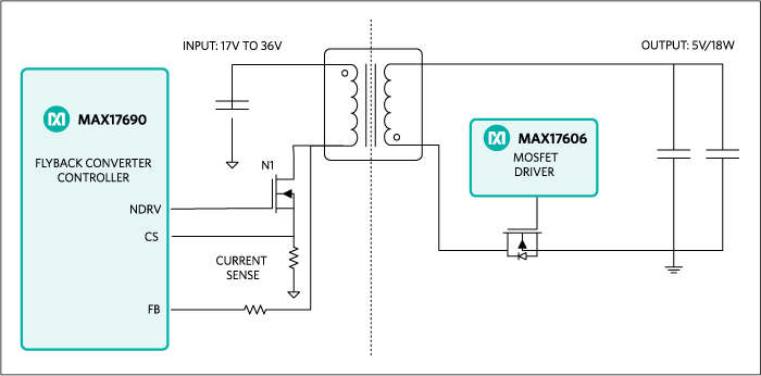
Figure 1. The MAXREFDES120# reference design block diagram
Required Equipment
- MAXREFDES120 board
- One 24V DC power supply
- One electronic load
- 1 voltmeter
- 1 ammeter
The MAXREFDES120 board is fully assembled and tested. Use the following steps to verify board operation.
- Turn off the power supply.
- Connect the positive terminal of the power supply to the VIN pin of the MAXREFDES120 board.
- Connect the negative terminal of the power supply to the GND pin of the MAXREFDES120 board.
- Connect the VOUT connector of the MAXREFDES120 board to the positive terminal of the electronic load.
- Connect the negative terminal of the electronic load to the positive terminal of the ammeter.
- Connect the negative terminal of the ammeter to the GNDO connector of the MAXREFDES120 board.
- Connect the voltmeter across the VOUT and the GNDO connectors of the MAXREFDES120 board.
- Turn on the power supply.
- Set the electronic load to a constant current between 50mA to 2500mA.
- Verify the second voltmeter reading is 5V ±0.15V.
Lab Measurements
The MAXREFDES120 design was verified and tested under full input range and different output load conditions. The power efficiency vs. load current is illustrated in Figure 2.
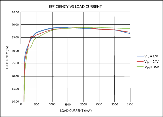
Figure 2. Power efficiency vs. load current
Figure 3 displays the output ripple at full load (ripple + spike is 180mVP-P) when the input is 24V.
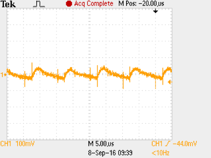
Figure 3. Output ripple at 2.5A load, 5VOUT.
Figure 4 displays the load transient response when the load is stepped from 200mA to 1.2A, and then dropped back to 200mA again. The output transient spike is about 200mV. The input is 24V and output is 5V.
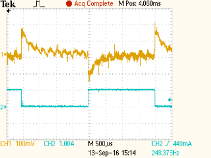
Figure 4. Transient response when load steps from 200mA to 1.2A
Figure 5 shows the load transient response when the load is stepped from 1.5A to 2.5A, and then dropped back to 1.5A again. The transient voltage is about 200mV. The input is 24V, and the output is 5V.
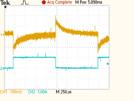
Figure 5. Transient response when load steps from 1.5A to 2.5A.
Documentation & Resources
-
MAXREFDES120 Design Files2021/02/15ZIP19 M
Support & Training
Search our knowledge base for answers to your technical questions. Our dedicated team of Applications Engineers are also available to answer your technical questions.