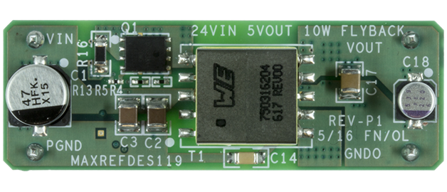
MAXREFDES119
Isolated 24V to 5V, 9W No-Opto Flyback Power Supply


Overview
設計リソース
説明
Analog's power supply experts have designed and built a series of isolated, industrial power-supply reference designs. Each of these power supplies efficiently converts 24V into useful voltage rails at a variety of power levels. Every power rail is isolated with a readily available transformer from multiple, global vendors, providing for quick, convenient transformer selection. Each design has been tested for load and line regulation, as well as efficiency and transient performance.
MAXREFDES119 is unique. While most isolated power supplies require an optocoupler, MAXREFDES119 does not use one. The design features the MAX17690, a peak-current-mode converter with flexible switching frequency, which measures primary-side voltage for system control, and the MAX17606, a secondary-side MOSFET driver that eliminates inefficient diodes. This efficient flyback topology provides a 5V output at 9W of power (1.8A) from a 24V input. This entire circuit fits on a 20mm (0.8in) x 60mm (2.35in) board.
機能と利点
- Functional insulation
- Compact and flexible
- Minimal external components
- Robust operation in adverse industrial environments
- 5V 1.8A with 20% over range current
- ±5% output accuracy
Details Section
Isolated power supplies provide reliable power regulation for a variety of applications. The MAXREFDES119 is a compact 24V input no-opto flyback converter module with a secondary-side synchronous MOSFET driver that features 5V at 1.8A output. Through-hole pins on the bottom side of the module allow quick and easy integration of this power converter into any system requiring an isolated rail. Pins are 15.24mm (0.6in) from power to ground, and 50.8mm (2in) from the input side to the output side.
The MAX17690 is a no-opto peak-current-mode controller for design of wide input-voltage flyback and boost regulators. The reference design operates over a 17V to 36V input voltage range, and provides up to 1.8A (plus 20% overhead) at 5V output. The design is set to switch at 90kHz, but the switching frequency of the controller is programmable from 50kHz to 250kHz. This allows for optimization of filter components, resulting in compact and cost-effective power conversion. With primary-side feedback, an opto-coupler or third winding is not needed to derive a feedback signal across the isolation barrier.
The input undervoltage lockout (EN/UVLO) is provided for programming the input-supply start voltage (set to 17V in the design), and to ensure proper operation during brownout conditions. The EN/UVLO input is also used to turn on/off the IC. The overvoltage input (OVI) protection scheme is provided to make sure that the controller shuts down when the input supply exceeds its maximum allowed value (set to 36V in the design).
A capacitor is connected to the SS pin to program the soft-start period, hence reducing the input inrush current during startup. Hiccup-mode overcurrent protection and thermal shutdown are provided to minimize dissipation in overcurrent and overtemperature-fault conditions.
On the secondary side, a MOSFET replaces the diode typically used in a flyback converter, with the MAX17606 acting as the MOSFET driver. By replacing the secondary diode with a MOSFET, the overall converter efficiency improves, which simplifies thermal management.
The reference design delivers a peak efficiency of 90% with the supplied components when the input is 24V. This general-purpose power solution can be used in many different types of power applications, such as programmable logic controllers (PLC), industrial process control, industrial sensors, telecom power supplies, isolated battery chargers, servers, and embedded computing.

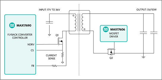
Figure 1. The MAXREFDES119 reference design block diagram.
The MAXREFDES119 reference design contains all the control circuitry and electric components required for designing a 17V to 36V wide-input, 5V 9W output isolated-flyback converter power supply.
When the primary-side MOSFET (Q1) is turned on, current flows through the primary winding of the transformer, which stores the energy. The CS-pin input and the current-sense resistor set the peak-current limit and provide overcurrent protection. When Q1 is turned off, the energy stored in the primary side of the transformer is transferred to the secondary side. The MAX17690 samples the output voltage by sensing the voltage of the transformer on the primary side.
The secondary side of the circuit consists of a MOSFET (Q2), a MAX17606 MOSFET driver, and several output capacitors. The MOSFET on the secondary side emulates the diode in typical flyback-converter applications. With the Q2 source connected to GND, the MAX17606 senses the voltage at the drain pin of Q2 to determine the timing for turning on/off the MOSFET. When Q1 is off and the drain voltage of Q2 on the secondary side becomes less than -100mV, the MAX17606 turns on Q2. Thus, the transformer pushes the current to the load at the output and the remaining energy is stored in the output capacitors. On the contrary, when Q1 is on and the drain voltage of Q2 becomes more than 30mV, the MAX17606 turns off Q2 to prevent current flow back into the transformer, while the output capacitors discharge to the load.
The MAXREFDES119 system requires 2% of full load (about 40mA) for the output to regulate within limits. When the load is lower than 2%, the output is clamped by a 5.6V Zener diode.
Startup Voltage and Input Overvoltage Protection Setting (EN/UVLO, OVI)
The EN/UVLO pin in the MAX17690 serves as an enable/disable input, as well as an accurate programmable undervoltage lockout (UVLO) pin. The MAX17690 does not begin startup operation unless the EN/UVLO pin voltage exceeds 1.21V (typ). The MAX17690 turns off if the EN/UVLO-pin voltage falls below 1.09V (typ). A resistor-divider from the input DC-bus-to-ground can be used to divide down and apply a fraction of the input DC voltage to the EN/ UVLO pin. The values of the resistor-divider can be selected so that the EN/UVLO-pin voltage exceeds the 1.21V (typ) turn-on threshold at the desired input DC-bus voltage. The same resistor-divider can be modified with an additional resistor (ROVI) to implement overvoltage-input protection in addition to the EN/UVLO functionality. When the voltage at the OVI pin exceeds 1.21V (typ), the MAX17690 stops switching. Switching resumes with soft-start operation, only if the voltage at the OVI pin falls below 1.09V (typ). For the expected values of the startup DC-input voltage (VSTART) and overvoltage-input protection voltage (VOVI), the resistor values for the divider can be calculated as follows:

Figure 0
Procedure
The MAXREFDES119 board is fully assembled and tested. Use the following steps to verify board operation.
- Turn off the power supply.
- Connect the positive terminal of the power supply to the VIN pin of the MAXREFDES119 board.
- Connect the negative terminal of the power supply to the PGND pin of the MAXREFDES119 board.
- Connect the VOUT connector of the MAXREFDES119 board to the positive terminal of the electronic load.
- Connect the negative terminal of the electronic load to the positive terminal of the ammeter.
- Connect the negative terminal of the ammeter to the GNDO connector of the MAXREFDES119 board.
- Connect the voltmeter across the VOUT and the GNDO connectors of the MAXREFDES119 board.
- Turn on the power supply.
- Set the electronic load to a constant current between 0mA to 2000mA.
- Verify with the voltmeter reading is 5V ±0.15V.
- Power down the design in the reverse order: Turn-off electronic load, and then the power supply.
Lab Measurements
The MAXREFDES119 design was verified and tested under full-input range and different output-load conditions.
The power efficiency vs. load current is illustrated in Figure 2.

Figure 2. Power efficiency vs. load current
Figure 3 display the output ripple at full load (ripple + spike is 117mVP-P) when the input is 24V.

Figure 3. Output ripple at 1.8A load, 5VOUT
Figure 4 displays the load transient response when the load is stepped from 50mA to 720mA, and then dropped back to 50mA again. The output transient spike is about 250mV. The input is 24V and output is 5V.

Figure 4. Transient response when load steps from 5mA to 720mA
Figure 5 shows the load transient response when the load is stepped from 1.08A to 1.8A, and then dropped back to 1.08A again. The transient voltage is about 210mV. The input is 24V, and the output is 5V.

Figure 5. Transient response when load steps from 1.08A to 1.8A.
| Part Number | Transformer Vendor | Transformer Part Number |
| MAXREFDES119A | Wurth | 750316204 |
| MAXREFDES119B | Sumida | 14354T015 |
| MAXREFDES119C | HanRun | HR051449 |
Documentation & Resources
-
MAXREFDES119 Design Files2021/02/15ZIP19 M
Support & Training
Search our knowledge base for answers to your technical questions. Our dedicated team of Applications Engineers are also available to answer your technical questions.