MAXREFDES1161
MAXREFDES1161: Small Form Factor, High Accuracy, 2-Wire, 4–20mA Current Loop Transmitter


Overview
設計リソース
説明
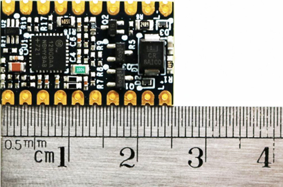
The MAXREFDES1161 is a small form factor, high accuracy, 2-wire 4–20mA transmitter which integrates all functional and protection blocks in a small 1.0in x 0.6in dual-row header footprint that is compatible with breadboards and off-the-shelf peripheral expansion boards.
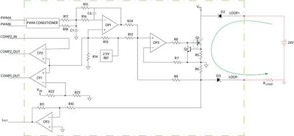
The MAXREFDES1161 uses the MAX12900 to achieve a total solution for industrial loop-powered current transmitters which convert the microcontroller 16-bit pulse-width modulated (PWM) signal to current without using a DAC, greatly reducing total system cost without degrading the accuracy. The 4–20mA current loop transmitter can achieve a 1μA resolution and 0.1% FS accuracy. The MAX12900 also provides diagnostic functionality, such as loop power monitoring and current readback. The reference design integrates protection functions, such as loop power reverse protection and overvoltage protection, and can support up to 36V loop power input at 4mA current output.
The MAXREFDES1161 can be used to evaluate the performance of the MAX12900 and can be directly used in final products to simplify the current loop transmitter design and shorten development cycles.
機能と利点
- Loop Compliance Voltage up to 36V
- 4–20mA Output with 0.1% FSR Accuracy
- Robust Industrial Design with Reverse Voltage Protection, and Overcurrent Protection
- IEC 61000-4 Transient Immunity Protection
- Industrial Standard Form Factor
- Complete solution with Proven Layout
使用されている製品
Details Section
The MAXREFDES1161 uses dual PWM signals to control the current loop output. PWMA is an 8-bit coarse signal adjustment, and PWMB is an 8-bit fine signal adjustment. The MAX12900 internal general-purpose amplifier (OP1) acts as a multi-feedback low pass filter (LPF) to convert the PWM conditioner output to a DC analog signal used to control the current output. The control loop consists of a low drift amplifier (OP3) and an external transistor (Q1) (Infineon® IRLML0100TRPBF). Another general-purpose amplifier (OP2) is used to readback the loop current value to provide an output signal (IOUT), which can be connected to the microcontroller ADC input to remotely monitor the loop current value. The low drift 2.5V voltage reference within the MAX12900 is used to generate an offset current output and provides a comparator reference voltage for CP1 and CP2. One comparator (CP1) is configured as a loop power supply voltage monitor, and the second comparator (CP2) is reserved for general purpose monitoring. Both comparator outputs (COMP1_OUT and COMP2_OUT) and CP2’s inverting input are connected to pads at the board edge.
Step 1: PWM to DC Conversion
The MAX12900 PWM conditioner circuits can accept two PWM signals from the microcontroller: one for coarse PWM (PWMA) and the other for fine PWM (PWMB). The output voltage of the PWM conditioner circuit reflects the PWM input with the output high level at the reference voltage and the low level at GND. This reduces the requirement for PWM input logic levels. The PWM output feeds into the low-pass filter (LPF) to generate a DC voltage used to control the current output. Amplifier OP1 and external components consist of the multi-feedback LPF. The coarse gain is set to 1 by using a 22.6kΩ gain resistor (R17) and a 22.6kΩ feedback resistor (R15), while the fine gain is set to 1/66 by using a 1.5MΩ gain resistor (R18). The two PWM outputs are summed using the feedback resistor (R15) of OP1. This configuration can achieve an equivalent 14-bit resolution signal path. The coarse PWM is 8 bits while fine PWM is 6 bits in equivalent resolution.
The OP1 is configured as an inverting amplifier with the non-inverting input connected to VREF/2. OP1 output is calculated using the following equation:

where R15 and R17 are 22.6kΩ, R18 is 1.5MΩ, R15/R18 is 1/66, and PWMA and PWMB correspond to their DC output, which is calculated as follows:
PWMA/B=DutyCycleA/b×VREF
The formula can be simplified as follows:

During power-up, the PWMA and PWMB inputs can float before the microcontroller is initialized. If the PWM inputs are low, the OP1 output settles at approximately VREF, driving the maximum loop current output. To avoid this, it is recommended to add pullup resistors on the PWMA and PWMB inputs to ensure the loop current output is minimal during power-up.
The maximum PWM input frequency depends on the PWM conditioner’s minimum input pulse width. For the MAX12900, the minimum input pulse width is 390ns. The PWM is an 8-bit counter with values between 0 to 255, so the maximum PWM input frequency can be calculated as follows:
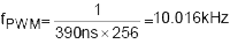
For the MAXREFDES1161#, the PWM frequency is 10kHz. Decreasing the PWM frequency introduces noise in the current loop and is not recommended.
Step 2: 4–20mA Current Loop Control Panel
The current loop control consists of an amplifier (OP3), a transistor (Q1) (Infineon IRLML0100TRPBF), and other external passive components as shown in Figure 2.
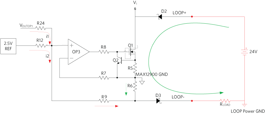
Figure 2. MAXREFDES1161 control loop
The amplifier OP3 inverting input is connected to the MAX12900 GND through the resistor R7. Because of the high input impedance of OP3, there is effectively no current flowing through R7, and hence the inverting input of OP3 is effectively held at the MAX12900 GND level. There are two inputs at the OP3 non-inverting input: the 2.5V reference voltage with R12 in series and the OP1 output (VOUTOP1) with R24 in series. OP3 is an ultra-low offset voltage amplifier, so the voltage level is the same for the two OP3 inputs. Since the OP3 non-inverting input is also held at the MAX12900 GND level, the current I1 is VOUTOP1/R24 and current I2 is VREF/R12. The constant current I2 is called the offset current. I1 is called the control current and is controlled by VOUTOP1. Both I1 and I2flow through R9 and generate a voltage drop on R9, which equals to (I1+I2)×R9. This voltage drop on R9 forces a current to flow through the sense resistor (R6) generating the loop current, which can be calculated using the following equation:
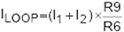
On the MAXREFDES1161#, R9=24.9kΩ, R6=24.9Ω, R12=1MΩ, and R24=100kΩ, giving
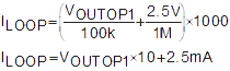
The offset current is 2.5mA, and the loop current is directly controlled by VOUTPUT1, which is the voltage output from the PWM conditioner circuit. Therefore, the PWM input also directly controls the loop current. This control is achieved by the OP3 output controlling the VGS of Q1 to limit the current flowing through Q1. The voltage drop on Q1 depends on the loop load (RLOAD) and the loop current and is calculated with the following equation:
VQDROP=VLOOP-2×VDIODE-ILOOP×(R5+R6+RLOAD)
where RLOAD=100Ω, ILOOP=20mA, and VLOOP=24V. The voltage drop on Q1 is approximately 19V, and the power dissipation of Q1 is calculated as follows:
PQ1=20mA×19V=0.38W
The maximum power dissipation of Q1 at 125°C is about 0.25W, so two MOSFETs are connected in parallel (Q1 and Q3) to increase the power dissipation and ensure operation at 125°C.
Step 3: Loop Load Consideration
A sense resistor (R6) is connected between the “MAX12900 GND” and D3 on LOOP-, and the loop load resistor (RLOAD) is connected between LOOP- and the loop ground (GND).
If the loop load is too large, the voltage between VIN and the MAX12900 GND becomes lower than the MAX12900 minimum operation voltage of 4V. The maximum load for 24V loop power is calculated by the following equation:
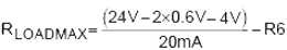
The maximum load for the reference design is 900Ω at 24V loop power supply. Increase the loop power supply voltage to meet the 4–20mA maximum loop load requirement of 1kΩ, but also make sure the power dissipation of MOSFETs Q1 and Q3 can operate over the full temperature.
Step 4: Transient Immunity Protection
To prevent high voltage transient pulses at the LOOP power supply inputs from damaging the MAX12900, a transient voltage suppressor (TVS) device (D1, 36V TVS SMBJ36CA) is used to clamp the input voltage to below 36V to protect the internal circuitry. Two diodes (D2 and D3, PMEG6002ELD) are connected between LOOP+ and LOOP- for reverse loop power supply protection. In addition, overcurrent protection is provided using a bipolar transistor (Q2, BC846BW) and R5 connected to the Q1 and Q3 source pin, which turns on Q2, reduces Q1 and Q3 VGS, and effectively clamps the loop current to 30mA during a fault condition.
Step 5: Diagnostic Circuit
OP2 is configured as an inverting amplifier, where the gain is set by resistor R10 and R11 to be equal to 4. The output voltage of the amplifier is calculated by the following equation, where ILOOP is in the 4–20mA range:
VOUTOP2=4×24.9×ILOOP=100×ILOOP
The output of OP2 (IOUT) can be connected to the microcontroller with an integrated ADC to read back the voltage that is proportional to the loop current, and action can be taken if it is different than the desired value.
There are two comparators in the MAX12900 (CP1 and CP2), which can be used as voltage monitors. In the MAXREFDES1161#, the non-inverting input of the comparators is VREF/2 or 1.25V nominal. The inverting input of CP1 is connected to a voltage divider (R22 and R23) to monitor the MAX12900 power supply voltage VIN. The inverting input of CP2 is reserved and connected to a pad at the PCB edge.
Step 6: Power Supply
The reference design is powered by the loop power supply connected across LOOP+ and LOOP-, which is nominally a 24V supply. The resistor R2 helps inhibit the inrush current during power-on and connects to the input of the internal LDO that generates a 3.3V VCCI to power the MAX12900. External resistors R3 and R4 are used to set a feedback voltage to define the LDO output voltage. The power-up sequencer keeps all op-amp and PWM outputs at high impedance and the outputs of the comparators low during power-up until VCCI reaches 90% of its final value. The PWRGOOD signal is delayed by 0.7ms after VCCI reaches 90% of its final value. The external components, such as a sensor or a microcontroller, must not draw current from VCCI before the PWRGOOD signal is asserted. In this design, the PWRGOOD signal is used as a switch control signal to control the power supply to the external components. The DMC2004DWK dual MOSFET (U2) acts as a switch to use PWRGOOD as the control signal between VCCI and VCCI_OUT. VCCI_OUT also connects to the MAX12900 VDD pin, which is the power supply for comparators CP1 and CP2. Refer to the MAX12900 data sheet for further details of the individual blocks.
Step 7: External Resistor Selection
To ensure the loop current has low drift and high accuracy, the external passive components such as gain setting resistors and sense resistors are specified for high accuracy and low drift. The MAXREFDES1161 uses resistors with ratings of 0.1% accuracy and 10ppm or 25ppm for low temperature drift. For more details about the resistor selection, see the bill of materials.
Documentation & Resources
-
MAXREFDES1161 Design Files2021/03/03ZIP822 K
Support & Training
Search our knowledge base for answers to your technical questions. Our dedicated team of Applications Engineers are also available to answer your technical questions.