Low input voltage operation of an LED backlight driving system using MAX25014
要約
This application note describes the operation of the MAX25014 4-Channel Backlight High Brightness LED driver at low input voltage. The resulting issues and proper component selection guidelines are introduced along with a comparison between theoretical calculations and bench measurements. This application note focuses on the boost converter topology.
Introduction
This application note details a low-input voltage application for the MAX25014 4-Channel Backlight High-Brightness LED driver. It proposes an efficiency calculation, which considers contributions both from the IC and external components, and suggests how to reduce power losses in this condition. The MAX25014 is a peak current-mode-controlled LED driver, which can drive up to four LED strings in different configurations. This application note focuses on its boost topology, in which the LED string forward voltage is always higher than the input supply voltage range. It is assumed that the LED driver is always kept in the continuous-conduction mode (CCM).
The MAX25014 offers several features: four integrated current outputs that can sink up to 149mA LED current each, integrated spread-spectrum and phase shifting, I2C-controlled pulse-width modulation (PWM) dimming and hybrid dimming, and programmable switching frequency between 400kHz and 2.2MHz. The device can operate down to 2.5V power supply after startup.
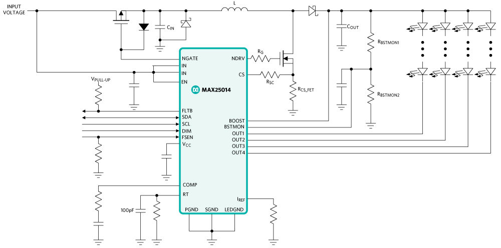
Figure 1. Typical MAX25014 operating circuit.
Low-Input Voltage Boost Converter Operation and Efficiency
Some preliminary definitions of LED driver parameters must be introduced before analyzing the boost converter behavior at low-input voltage.
The total output current (ILED) needed to drive the LED strings is:
where ISTRING is the current per string and NSTRING is the number of strings.
The voltage needed to drive the LED strings (VLED) is:
where VOUT_ refers to the OUT_ pin regulation voltage (equal to 1V approximately), VF is the typical expected forward drop on each LED, while NLED is the number of LEDs in each string.
The duty cycle (D) calculation is then straightforward:
where VD is the forward drop of the rectifying diode (approximately 0.6V) and VIN is the input-supply voltage in volts.
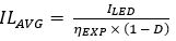
Including the expected converter's efficiency (ηEXP) at a defined input voltage value, the duty cycle and LED current determine the average inductor current (ILAVG) as:
Now that the average inductor current is determined, the peak inductor current (ILP) is:
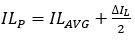
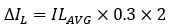
where ΔIL is the peak-to-peak inductor current ripple in amperes (A). Considering typically ±30% of the average inductor current as the maximum peak-to-peak ripple, ΔIL is:
The MAX25014, like most boost regulators, uses an internal LDO voltage regulator powered from the input of the device to provide lower voltage power to the analog and digital control circuitry within the IC.
The MAX25014 can maintain a VCC = 5V drive for the external MOSFET by switching the LDO regulator input from the input to the output of the boost converter when the former drops below the 5.8V (typ) switchover threshold. This prevents the LDO output voltage from collapsing, which limits the ability of the gate driver to properly enhance the external MOSFET. It consequently makes it operate in a higher resistance state causing higher power dissipation in the form of heat as current is passed through the device. Alternately, the power dissipated by the LDO itself becomes higher at the low-input voltage, as shown in a later section.
Power losses related to heat dissipation from the low-side MOSFET's drain-to-source resistance (PRDSON) are called conduction losses.
Switching losses from the low-side MOSFET and high-side diode (PSW, M and PSW, D) must also be considered besides conduction losses: these losses increase as the boost switching speed increases. So, when the programmed switching frequency is higher than 1MHz, the MAX25014 lowers it by 30% when the input voltage is below the switch-over voltage to reduce heat dissipation.
The described features are implemented in the IC, since at very low-input voltages and high switching frequency, the efficiency of the boost converter reduces, and the input current can reach very high levels. Consequently, the MOSFET total losses can become severe and generate considerable heat.
The inductor is another significant contributor to power losses in addition to the external switch. The inductor total loss (PL) can be split into ohmic and core losses. The former is related to the winding resistance of the inductor (RDCR) while the latter directly depends on the switching frequency. It cannot be easily modeled without knowing the core material characteristics in detail and is neglected in this analysis. The inductor's winding capacitance is also ignored in subsequent paragraphs.
The conduction losses from the NGATE protection switch (PNGATE) and the freewheeling diode (PDIODE) conclude the analysis on power dissipation from external components. All the above factors are summed up to yield the total external losses (PEXT):

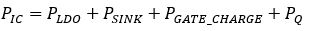
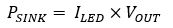
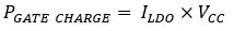
Power dissipation from the IC itself must also be considered though it has a minor impact on the overall system efficiency. The main losses come from the integrated voltage regulator block (PLDO), current sinks (PSINK), gate charge (PGATE_CHARGE), and quiescent current consumption (PQ), and form the total IC losses (PIC) as:
(Eq. 1), (Eq. 2), (Eq. 7), and (Eq. 8) together calculate the converter's efficiency (η) as:

Once η is calculated, the efficiency corrective factor in Eq. 4 must be iteratively updated, by setting ηEXP = η, to obtain a more and more accurate value for ILAVG until the two efficiency values match.
Detailed Description of Power Loss Factors
This part describes how to obtain the power dissipation for each component. Starting from the IC losses, it is first necessary to calculate the average value of current required by the internal LDO regulator:
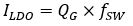
where QG is the total gate charge of the chosen external MOSFET switch and fSW is the converter's switching frequency.
The power dissipated by the internal voltage regulator is then:


The current sinks, gate-charge, and quiescent or standby consumption losses are respectively calculated as:
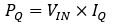
The value of the IC's quiescent current, IQ, can be retrieved from the device's EC table in the MAX25014 data sheet.
The conduction losses related to the external components mentioned in the previous section are given by the following equations:


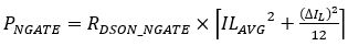
RDSON_NGATE in Eq. 19 is the drain-to-source resistance of the NGATE protection switch.
A crude estimate of the MOSFET's switching losses can be calculated using simplified linear approximations of the gate-drive current, drain current and drain voltage waveforms:
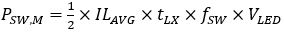
tLX can be estimated considering the gate-drive currents during two different switching transitions of the MOSFET's turn-on procedure:
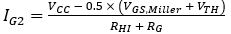
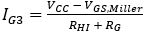
IG2 current charges the input capacitor of the device from VTH to VGS,Miller, and IG3 current discharges the Crss capacitor while the drain voltage is dropping from VLED to 0V. The VGS,Miller and VTH parameters are found in the selected MOSFET's data sheet, RHI is the gate driver's high-side resistance (the value is indicated in the MAX25014 data sheet), and RG is the sum of the MOSFET's internal and external gate resistors.
The two switching transition times are then:
The CISS and CRSS capacitances are also MOSFET-specific parameters and their typical values can be found in the device's data sheet. The sum of t2 and t3 leads to the required tLX time:

The switching losses on the rectifying diode, which occur in the transitions from the conducting to nonconducting states, are known to be lower than those on the MOSFET and, to a first approximation, are considered as:

Comparing the Numerical Simulation and Bench Test Results
The formulas introduced in the last paragraph theoretically evaluate the MAX25014 boost converter efficiency at different input voltages. The numerical results were compared to efficiency measurements performed on a MAX25014 evaluation board driving four 8- and 9-LED strings with a constant current of 120mA each at 2.2MHz switching frequency. It was assumed that each LED had a typical expected forward voltage drop and the LED driver circuit had to be fed by a 12V to 4V input voltage. The values and part numbers of the main external components used on the evaluation board are shown in Figure 2.
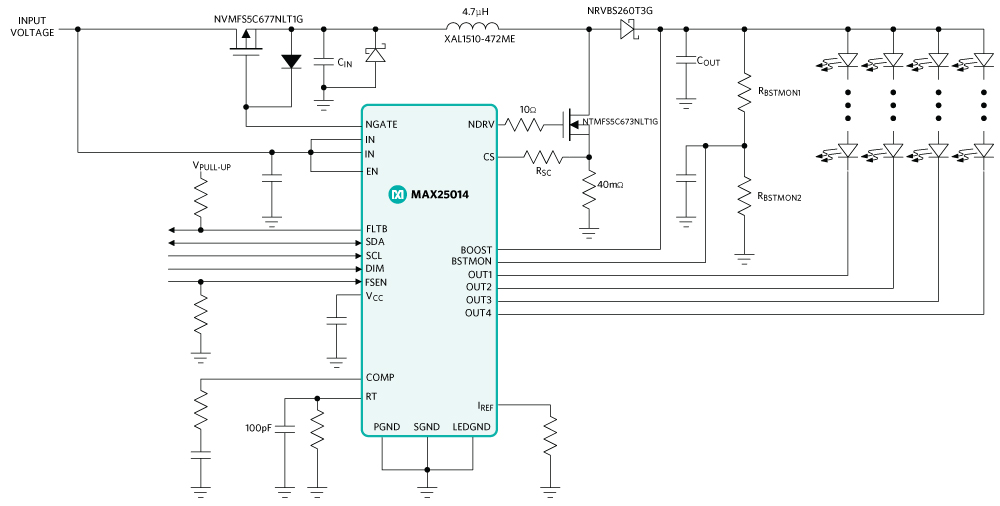
Figure 2. Typical MAX25014 operating circuit.
The component-specific values used for the numerical simulations, aside from those already shown in Figure 2, are listed in Table 1.
| Electrical PARAMETERS | Values |
|---|---|
| QG – NTMFS5C673NLT1G | 4.5nC |
| VGS,Miller – NTMFS5C673NLT1G | 2.9V |
| VTH – NTMFS5C673NLT1G | 1.6V |
| CISS – NTMFS5C673NLT1G | 880pF |
| CRSS – NTMFS5C673NLT1G | 11pF |
| IQ – MAX25014 | 9.5mA |
| RHI – MAX25014 | 1.5Ω |
| RDCR – XAL1510472ME | 9mΩ |
| RDSON – NTMFS5C673NLT1G | 13mΩ |
| RDSON_NGATE – NVMFS5C677NLT1G | 21.5mΩ |
Figures 3 and 4 show the results of the efficiency comparisons in the two cases.
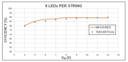
Figure 3. MAX25014 efficiency vs. input voltage, 8 × 4 LEDs, fsw = 2.2MHz.
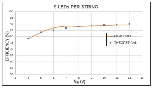
Figure 4. MAX25014 efficiency vs. input voltage, 9 × 4 LEDs, fsw = 2.2MHz.
Conclusion
This application note introduces the main factors that contribute to the boost efficiency of the MAX25014 with emphasis on how this device behaves on applying a low-input voltage.
The estimation of the overall power losses, though an approximation of the first order, has a good match with the bench measurements.