DS26303ショートホールラインインタフェースユニットとLXT384
要約
この文書では、既存のLXT384アプリケーションでDS26303を使うために必要となる情報に重点をおきつつ、DS26303とLXT384の違いについて説明します。機能の違い、レジスタの考慮点、およびハードウェアの考慮点についての説明を提供します。
はじめに
この文書では、既存のLXT384アプリケーションでDS26303を使うために必要となる情報に重点をおきつつ、DS26303とLXT384の違いについて説明します。DS26303は、3.3V単一電源で動作してE1/T1/J1をサポートする、8チャネルのショートホールラインインタフェースユニット(LIU)です。このデバイスは、ソフトウェアの変更なしでLXT384の機能をサポートするとともに、新たに追加されたレジスタバンクを使用することによって利用可能になった追加機能を提供します。DS26303は、PCBのレイアウトを変更することなく、希望のアプリケーションに合わせて単に外付け部品の値を変えるだけで、既存のLXT384アプリケーションで使用することができます。
機能の違いは、3つのセクションに分けて説明します。表1では、DS26303の機能の中でLXT384には存在しないものの一覧を示します。表2では、LXT384の機能の中でDS26303には存在しないものの一覧を示します。表3では、DS26303とLXT384の両方に存在しており、かつ両方のデバイスで同じ実装になっていない機能の一覧を示します。
DS26303とLXT384のレジスタの違いについては、DS26303の拡張レジスタセットによって提供される追加機能と合わせて、表6~表10で説明します。図1と表11では、DS26303を既存のLXT384アプリケーションで使用する場合に必要となる、部品の値の細かな変更について示します。
表1. LXT384には存在しないDS26303の機能
| DS26303 | LXT384 |
| Programmable options to clear interrupt status on write or read. Clear on read is default. | Not supported. |
Individual channel control for jitter attenuator:
|
All channels have global control. |
| Internal software-selectable transmit and receive side termination for 100Ω T1 twisted-pair, 110Ω J1 twisted-pair, 120Ω E1 twisted–pair, and 75Ω E1 coaxial applications. | Not supported. |
| In HPS mode, the transmitter output and the internal impedance of the receiver can be turned off with only the OE pin. | Requires that both receivers use the same front-end termination. |
| Built-in BERT tester for diagnostics. | Not supported. |
Individual channel control for:
|
All channels have global control. |
| Individual channel-line violation detection. | Not supported. |
| Flexible MCLK See Table 4 for available input frequencies. |
Not supported. |
| Programmable TECLK output pin (1.544MHz or 2.048MHz) | Not supported. |
| Programmable CLKA output pin See Table 5 for available output frequencies. | Not supported. |
| Flexible interrupt pin | Not supported. |
表2. DS26303には存在しないLXT384の機能
| DS26303 | LXT384 |
| Uses single optimal value. | Capability to select the jitter attenuator bandwidth. |
| — | Analog JTAG |
| MLCK Pin Functionality The DS26303 and LXT384 both require MCLK to for data with clock recovery as well as AIS detection. The MCLK pin of the LXT384 provides additional functionality not present in the DS26303. LXT384 MCLK held high.
|
|
表3. DS26303とLXT384の間における機能の相違
| DS26303 | LXT384 |
| 3.3V LIU power only, 5V not provided. | 5V LIU power. |
| Non-mux Intel® write address to WRB rising-edge setup time is 17ns. | Non-mux Intel write address to WRB rising-edge setup time is 6ns. |
| Expects non-mux Intel read address to be valid when RDB is active. | Non-mux Intel read address to RDB rising-edge setup time is 6ns. This might be an error in datasheet because data is out before this setup time. |
| Inactive RDY to tri-state delay time 12ns (max). | Inactive RDY to tri-state delay time 3ns (max). |
| Clears the interrupt pin when reading or writing the interrupt status. | Clears interrupt pin when reading the status register. |
| Jitter attenuator FIFO depths of 32 bits or 128 bits. | Jitter attenuator FIFO depths of 32 bits or 64 bits. |
Individual channel control for jitter attenuator:
|
All channels have global control. |
表4. DS26303のMCLKの選択
| PLLE | MPS1, MPS0 | MCLK MHz (±50ppm) | FREQS | T1 or E1 Mode |
| 0 | xx | 1.544 | x | T1 |
| 0 | xx | 2.048 | x | E1 |
| 1 | 00 | 1.544 | 1 | T1/J1 or E1 |
| 1 | 01 | 3.088 | 1 | T1/J1 or E1 |
| 1 | 10 | 6.176 | 1 | T1/J1 or E1 |
| 1 | 11 | 12.352 | 1 | T1/J1 or E1 |
| 1 | 00 | 2.048 | 0 | T1/J1 or E1 |
| 1 | 01 | 4.096 | 0 | T1/J1 or E1 |
| 1 | 10 | 8.192 | 0 | T1/J1 or E1 |
| 1 | 11 | 16.384 | 0 | T1/J1 or E1 |
表5. DS26303のクロックAの選択
| CLKA3 to CLKA0 | MCLK (Hz) |
| 0000 | 2.048M |
| 0001 | 4.096M |
| 0010 | 8.192M |
| 0011 | 16.384M |
| 0100 | 1.544M |
| 0101 | 3.088M |
| 0110 | 6.176M |
| 0111 | 12.352M |
| 1000 | 1.536M |
| 1001 | 3.072M |
| 1010 | 6.144M |
| 1011 | 12.288M |
| 1100 | 32k |
| 1101 | 64k |
| 1110 | 128k |
| 1111 | 256k |
レジスタの考慮点
DS26303には、4つの主なレジスタバンクが内蔵されています。
- プライマリレジスタ(DS26303およびLXT384)
- セカンダリレジスタ(DS26303のみ)
- 個別LIUレジスタ(DS26303のみ)
- BERTレジスタ(DS26303のみ)
DS26303のプライマリレジスタは、ほぼLXT384のレジスタと同じですが、1点だけ例外があります。LXT384では予約されていたレジスタアドレス1Fhが、DS26303では代わりにDS26303の追加レジスタバンク用のアドレスポインタ(ADDP)として使用されています。DS26303を既存のLXT384の代わりに使用する場合、アプリケーションソフトウェアの変更は必要ありません。表6に、DS26303とLXT384に含まれるプライマリレジスタの一覧を示します。
表6. DS26303とLXT384のプライマリレジスタ
| Address (Hex) | DS26303 | LXT384 |
| 00–15 | Primary Registers | Registers |
| 16–1E | Reserved | Reserved |
| 1F | ADDP (Address pointer for additional register banks). This register must be set to point to the desired register bank. 00h) Primary Bank AAh) Secondary Bank 01h) Individual LIU Bank 02h) BERT Bank |
Reserved |
DS26303の追加機能と柔軟性を利用するためには、LXT384アプリケーション向けに書かれたすべてのオリジナルソースコードに、新規コードを追加する必要があります。DS26303のADDPレジスタのアドレスは1F (16進)ですが、これはLXT384では予約アドレスになっています。ADDPは、異なるレジスタバンクにアクセスするためのポインタとして使用されています。表7に、DS26303のレジスタバンクの一覧と、希望のレジスタバンクにアクセスするために必要となるADDPの値を示します。
表7. DS26303のアドレスポインタのバンク選択
| ADDP7 to ADDP0 (Hex) | Bank Name |
| 00 | Primary Bank |
| AA | Secondary Bank |
| 01 | Individual LIU Bank |
| 02 | BERT Bank |
表8に、セカンダリレジスタバンクに含まれるレジスタの一覧を示します。また、個別LIUレジスタバンクに含まれるレジスタの一覧を表9に、BERTレジスタバンクに含まれるレジスタの一覧を表10に、それぞれ示します。
表8. DS26303のセカンダリレジスタバンク
| Address (Hex) | Register Name |
| 00 | Single-Rail Mode Select |
| 01 | Line-Code Selection |
| 02 | Not used |
| 03 | Receiver Power-Down Enable |
| 04 | Transmitter Power-Down Enable |
| 05 | Excessive Zero-Detect Enable |
| 06 | Code-Violation-Detect Enable Bar |
| 07–1E | Not used |
| 1F | Set to AAh for access to Secondary Register Bank |
表9. DS26303の個別LIUレジスタバンク
| Address (Hex) | Register Name |
| 00 | Individual JA Enable |
| 01 | Individual JA Position Select |
| 02 | Individual JA FIFO Depth Select |
| 03 | Individual JA FIFO Limit Trip |
| 04 | Individual Short-Circuit-Protection Disable |
| 05 | Individual AIS Select |
| 06 | Master Clock Select |
| 07 | Global-Management Register |
| 08–0F | Reserved |
| 10 | Bit-Error-Rate Tester Control Register |
| 12 | Line-Violation Detect Status |
| 13 | Receive Clock Invert |
| 14 | Transmit Clock Invert |
| 15 | Clock-Control Register |
| 16 | RCLK Disable Upon LOS Register |
| 1E | Global-Interrupt Status Control |
| 1F | Set to 01h for access to Individual LIU Register Bank |
表10. DS26303のBERTレジスタバンク
| Address (Hex) | Register Name |
| 00 | BERT Control Register |
| 01 | Reserved |
| 02 | BERT Pattern Configuration 1 |
| 03 | BERT Pattern Configuration 2 |
| 04 | BERT Seed/Pattern 1 |
| 05 | BERT Seed/Pattern 2 |
| 06 | BERT Seed/Pattern 3 |
| 07 | BERT Seed/Pattern 4 |
| 08 | Transmit-Error Insertion Control |
| 09–0A | Reserved |
| 0C | BERT Status Register |
| 0D | Reserved |
| 0E | BERT Status Register Latched |
| 10 | BERT Status Register Interrupt Enable |
| 11–13 | Reserved |
| 14 | Receive Bit-Error Count Register 1 |
| 15 | Receive Bit-Error Count Register 2 |
| 16 | Receive Bit-Error Count Register 3 |
| 17 | Receive Bit-Error Count Register 4 |
| 18 | Receive Bit Count Register 1 |
| 19 | Receive Bit Count Register 2 |
| 1A | Receive Bit Count Register 3 |
| 1B | Receive Bit Count Register 4 |
| 1C–1E | Reserved |
| 1F | Set to 02h for access to BERT Register Bank |
ハードウェアの考慮点
DS26303は、PCBのレイアウトを変更することなく、既存アプリケーションのLXT384を置き換えることができます。必要なのは、希望するアプリケーションに応じて、外付け部品の値を変更することだけです。DS26303の推奨ネットワーク終端回路を図1に、またDS26303の適切な終端に必要な各部品の値を表11に示します。
トランスミッタ
LXT384は、TTIPおよびTRING出力と直列に送信側に抵抗を必要とします。LXT384ではこれらの抵抗に、0Ω (T1 3.3Vモード)、11Ω (E1 75Ω同軸)、または11Ω (E1 120Ωツイストペア)であることが推奨されています。DS26303は抵抗を必要としないため、実装されている場合はすべてのモードにおいて0Ωにしてください。LXT384は、パルスシェーピングを使用しない場合、DCブロッキングコンデンサを必要とします。DS26303はDCブロッキングコンデンサを必要としないため、既存のLXT384アプリケーションのPCBに実装されている場合は、0Ωの抵抗に交換してください。
レシーバ
受信側では、LXT384は12.4Ω (T1 3.3Vモード)、9.31Ω (E1 75Ω同軸)、または15Ω (E1 120Ωツイストペア)の終端抵抗が必要です。DS26303は、外部インピーダンスモードを使用している場合、すべてのモードで15Ωの終端抵抗が必要です。DS26303のソフトウェア選択可能なインピーダンス整合モードを使用している場合は、これらの抵抗は必要ありません。LXT384はRTIPおよびRRING端子と直列に1kΩの抵抗が必要です。ソフトウェア終端/インピーダンス整合を希望する場合は、これらの1kΩ抵抗を0Ω抵抗に交換してください。
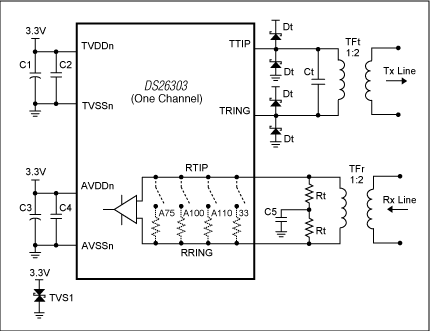
図1. LIUフロントエンド
表11. LIUフロントエンドの部品の値
| Mode | Component | 75Ω Coax | 120Ω Twisted Pair | 100Ω/110Ω Twisted Pair |
| Tx Capacitance | Ct | 560pF (typ). Adjust for board parasitics for optimal return loss. | ||
| Tx Protection | Dt | International Rectifier: 11DQ04 or 10BQ060 Motorola: MBR0540T1 | ||
| Rx Transformer 1:2 | TFr | Pulse: T1124 (0°C to +70°C) | ||
| Tx Transformer 1:2 | TFt | Pulse: T1114 (-40°C to +85°C) | ||
| Tx Decoupling (ATVDD) | C1 | Common decoupling for all eight channels is 68µF. | ||
| Tx Decoupling (ATVDD) | C2 | Recommended decoupling per channel is 0.1µF. | ||
| Rx Decoupling (AVDDn) | C3 | Common decoupling for all eight channels is 68µF. | ||
| Rx Decoupling (AVDDn) | C4 | Common decoupling for all eight channels is 0.1µF. | ||
| Rx Termination | C5 | When in external impedance mode, Rx capacitance for all eight channels is 0.1µF. Do not populate if using internal impedance mode. | ||
| Rx Termination | Rt | When in external impedance mode, the two resistors for all modes is 15.0Ω ±1%. Do not populate if using internal impedance mode. | ||
| Voltage Protection | TVS1 | SGS-Thomson: SMLVT 3V3 (3.3V transient suppressor) | ||
DS26303のその他の情報
マキシムの通信向け製品の詳細については、当社ウェブサイトのT/Eキャリアおよびパケット化製品から入手可能なデータシートをご覧ください。これらの通信デバイスの動作に関してさらにご質問がある場合は、テレコムアプリケーションサポートチームまでお問い合わせください。