Design Note 236: 1- and 2-Channel No Latency ΔΣ 24-Bit ADCs Easily Digitize a Variety of Sensors, Part 1
Since its introduction, the LTC2400 has transformed the method of designing analog-to-digital converters into a variety of systems. Some key features separating the LTC2400 from conventional high resolution ADCs are:
- Ultralow offset (1ppm), offset drift (0.01ppm/°C), full-scale error (4ppm) and full-scale drift (0.02ppm/°C) without user calibration
- Absolute accuracy less than 10ppm total (linearity + offset + full scale + noise) over the full operating temperature range
- Ease-of-use (eight pins, no configuration registers, internal oscillator and latency-free conversion)
- Low noise and wide dynamic range (0.3ppm RMS with VREF = VCC = 5V)
This two part Design Note introduces two new products lever aging the technology used in the LTC2400. Both parts are in tiny 10-pin MSOP packages. They include full-scale and zero-scale set inputs for removing systematic offset/full-scale errors. The first part (LTC2401) is a single-ended 1-channel device. The second part is a 2-channel device with automatic ping-pong channel selection (LTC2402).
The absolute accuracy and near zero drift of these devices enable several novel applications, of which two are presented in Part 1 and two in Part 2. The first application uses the full-scale set (FSSET) and zero-scale set (ZSSET) inputs of the 1-channel device (LTC2401) to digitize a half-bridge sensor. The second combines the LTC2402’s ping-pong channel selection, absolute accuracy and excellent rejection into a pseudo-differential bridge digitizer. The third (Part 2) is a thermocouple digitizer with a digital cold junction compensation scheme using the automatic ping-pong channel selection of the LTC2402 for simplified optical isolation. The final application (in Part 2) uses the LTC2402 to digitize an RTD temperature sensor and remove voltage drop errors due to long lead lengths using the second channel and the LTC2402’s underrange capabilities.
Single-Ended Half-Bridge Digitizer with Reference and Ground Sensing
Many types of sensors convert real world phenomena (temperature, pressure, gas levels, etc.) into a voltage. Typically, this voltage is generated by passing an excitation cur rent through the sensor. This excitation current also flows through parasitic resistors RP1 and RP2 (see Figure 1). The voltage drop across these parasitic resistors leads to systematic offset and full-scale errors.

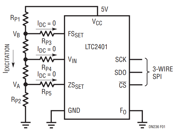
Figure 1. Half-Bridge Digitizer with Zero-Scale and Full-Scale Sense.
In order to eliminate the errors associated with these parasitic resistors, the LTC2401/LTC2402 include a full-scale set input (FSSET) and a zero-scale set input (ZSSET). As shown in Figure 1, the FSSET pin acts as a high impedance full-scale sense input. Errors due to parasitic resistance RP1 in series with the half-bridge sensor are removed by the FSSET input to the ADC.
The absolute full-scale output of the ADC (data out = FFFFFFHEX) will occur at VIN = VB = FSSET. Similarly, the offset errors due to RP2 are removed by the ground sense input ZSSET. The absolute zero output of the ADC (data out = 000000HEX) occurs at VIN = VA = ZSSET. Parasitic resistors RP3 to RP5 have negligible errors due to 1nA (typ) leakage current at the FSSET, ZSSET and VIN pins. The wide dynamic input range (–300mV to 5.3V) and low noise (0.6ppm RMS) enable the LTC2401 to directly digitize the output of the bridge sensor.
Pseudo-Differential Applications
Generally, designers choose fully differential topologies for several reasons. First, the interface to a 4- or 6-wire bridge is simple (it is a differential output). Second, they require good rejection of line-frequency noise. Third, they typically look at a small differential signal sitting on a large common mode voltage and need accurate measurements of the differential signal independent of the common mode input voltage. Many applications currently using fully differential analog-to-digital converters for any of the above rea sons may migrate to a pseudo-differential conversion using the LTC2402.
The LTC2402 interfaces directly to a 4- or 6-wire bridge, see Figure 2. Like the LTC2401, the LTC2402 includes a FSSET and a ZSSET for sensing the excitation voltage directly across the bridge. This eliminates errors due to excitation cur rents flowing through parasitic resistors. The LTC2402 also includes two single-ended input channels that can tie directly to the differential output of the bridge. The two conversion results may be digitally subtracted yielding the differential result.

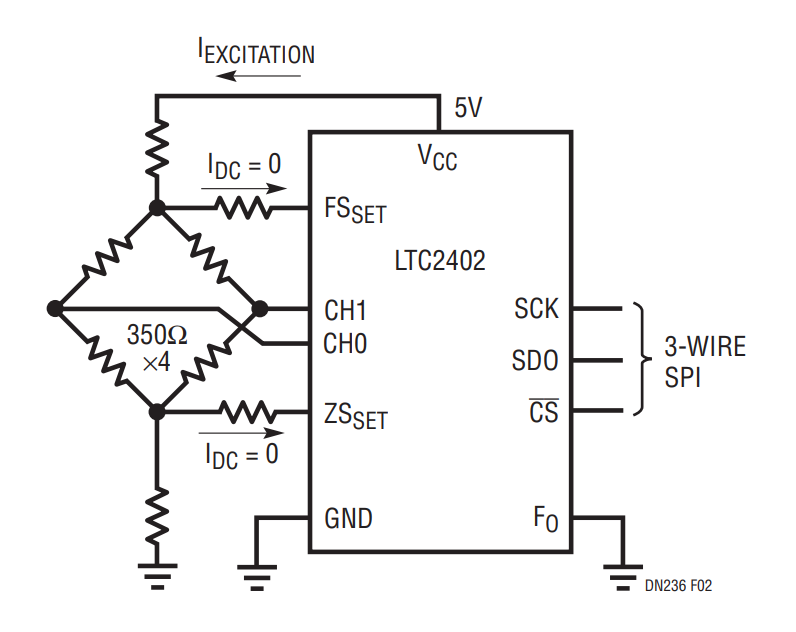
Figure 2. Pseudo-Differential Strain Gauge Application.
Additionally, the measurements from the individual channels represent the common mode output of the sensor. This information can be used to characterize and digitally compensate the temperature drift of the sensor.
Noise Rejection
The LTC2402’s single-ended rejection of line frequencies (50Hz/60Hz ±2%) and harmonics is better than 110dB. Since the device performs two independent single-ended conversions each with >110dB rejection, the overall common mode and differential rejection is much better than the 80dB rejection typically found in other differential delta-sigma converters.
In addition to excellent rejection of line frequency, the LTC2402 also exhibits excellent single-ended noise rejection of a wide range of frequencies due to its 4th order sinc filter, see Figure 3. Each single-ended con version independently rejects high frequency noise (>60Hz). Care must be taken to insure noise at frequencies below 15Hz and at multiples of the ADC sample rate (15,600Hz) are not present. For this application, it is recommended the LTC2402 is placed in close proximity to the bridge sensor in order to reduce the noise applied to the ADC input. By performing three successive conversions (CH0-CH1-CH0) the drift and low frequency noise can be measured and compensated for digitally.


Figure 3. Single-Ended LTC2401/LTC2402 Input Rejection.
著者
