DS26502のハードウェアモード
要約
DS26502のデータシートには、様々なアプリケーションにDS26502を実装するために必要なすべての情報が含まれています。データシートは、ソフトウェアモードのユーザを前提にして記述されています。このため、ハードウェアモードを使用するときには利用できない機能を有効にする制御レジスタを使用してDS26502をセットアップするために必要な情報が記載されています。
このアプリケーションノートには、ハードウェアモードにおけるDS26502の機能に焦点を絞った説明が記載されており、ソフトウェアモードを使用するときにしか利用することができないデータシートの情報は取り上げていません。
はじめに
DS26502には2つの主要な動作モードがあります。ソフトウェアモードとハードウェアモードです。「モード」とは、デバイスの機能を制御するために使われる方法のことです。ソフトウェアモードを実装したアプリケーションは、マイクロコントローラのシリアルバスまたはパラレルバスを使用して、DS26502に含まれる制御レジスタと通信します。ハードウェアモードでは、シリアル/パラレル通信バスの端子の機能を割り当て直し、端子の論理状態によってDS26502の内部機能を直接制御できるようにしています。
ハードウェアモードを使用する必要があるのはいつか?
DS26502をハードウェアモードで使用する利点は、機能を制御するためのマイクロコントローラが不要である点です。
それぞれのアプリケーションには、固有の要件があり、それによってハードウェアモードを使用するかどうかを決定します。設計者の主要な検討事項は、ソフトウェアモードでしか利用することができない機能のいずれかがアプリケーションで必要となるかどうかを決定することです。表1に、ハードウェアモードで利用することができないソフトウェアモードの機能を一覧で示します。DS26502データシートの完全な機能の説明を簡単に参照できるよう、レジスタのビット位置と名前を提供します。
ハードウェアモードの実装
ハードウェアモードでは、外部の端子によってDS26502の機能が制御されます。表2は、ソフトウェアモードのビット位置の機能とハードウェアモードでDS26502を制御するために使用する場合の対応する端子を表しています。
ソフトウェアで制御可能な機能の中には、ハードウェアモードで全面的に削除されているものもありますが、その他の機能は存在します。ただし機能を変更することはできません。変更することのできない機能を表3に示します。これらの機能は、ハードウェアモードを使用する標準的なアプリケーションで想定どおりに動作するよう慎重に選択したものです。ハードウェアモードでの各端子の機能全体についての説明を表4に示します。図1~図4は、ハードウェアモードにおけるDS26502の機能のブロック図です。このブロック図は、データシート内のソフトウェアモードでの対応するブロック図によく似ています。データシートに記載されているブロック図とは異なり、ここに示した図では、制御レジスタの代わりにDS26502の外部端子が記されています。ソフトウェアモードだけの機能も除外してあります。
DS26502アプリケーションのほとんどはソフトウェアモードを実装していますが、ハードウェアモードも依然として多くの顧客にとって実現可能な選択肢として存続しています。このアプリケーションノートをDS26502データシートと共に使用すれば、最小限の時間と労力で、ハードウェアモードでアプリケーションを動作させるために必要な情報が得られます。
| Register | Description |
| TSTRREG | Test Reset Register |
| IDR | Device Identification Register |
| INFO1 | Information Register 1 |
| INFO2 | Information Register 2 |
| IIR | Interrupt Information Register |
| SR1 | Status Register 1 |
| IMR1 | Interrupt Mask Register 1 |
| SR2.7 | Receive Yellow Alarm Clear Event |
| SR2.6 | Receive Alarm Indication Signal Clear Event |
| SR2.5 | Receive Loss Of Signal Clear Event |
| SR2.4 | Receive Loss of Frame Clear Event |
| SR2.3 | Receive Yellow Alarm Condition |
| IMR2 | Interrupt Mask Register 2 |
| SR3 | Status Register 3 |
| IMR3 | Interrupt Mask Register 3 |
| SR4 | Status Register 4 |
| IMR4 | Interrupt Mask Register 4 |
| INFO3 | Information Register 3 |
| RAF | Receive Align Frame Register |
| RNAF | Receive Non-Align Frame Register |
| RSiAF | Receive Si Bits of the Align Frame |
| RSiNAF | Receive Si Bits of the Non-Align Frame |
| RRA | Receive Remote Alarm |
| RSa4 | Receive Sa4 Bits |
| RSa5 | Receive Sa5 Bits |
| RSa6 | Receive Sa6 Bits |
| RSa7 | Receive Sa7 Bits |
| RSa8 | Receive Sa8 Bits |
| TEST1-16 | Test Register 1-16 |
| Position | Pin | Name |
| IOCR1.5 | RSM | RS_8K Mode Select |
| IOCR1.2 | TSM | TS_8K_4 Mode Select |
| T1RCR2.5 | HBE | Receive B8ZS Enable |
| T1TCR2.7 | HBE | Transmit B8ZS Enable |
| MCREG.7 | TMODE3 | Transmit Mode Configuration 3 |
| MCREG.6 | TMODE2 | Transmit Mode Configuration 2 |
| MCREG.5 | TMODE1 | Transmit Mode Configuration 1 |
| MCREG.4 | TMODE0 | Transmit Mode Configuration 0 |
| MCREG.3 | RMODE3 | Receive Mode Configuration 3 |
| MCREG.2 | RMODE2 | Receive Mode Configuration 2 |
| MCREG.1 | RMODE1 | Receive Mode Configuration 1 |
| MCREG.0 | RMODE0 | Receive Mode Configuration 0 |
| TPCR.1 | TCSS1 | Transmit Clock (TX CLOCK) Source Select 1 |
| TPCR.0 | TCSS0 | Transmit Clock (TX CLOCK) Source Select 0 |
| SR2.2 | RAIS | Receive Alarm Indication Signal |
| SR2.1 | RLOS | Receive Loss Of Signal Condition |
| SR2.0 | RLOF_CCE | Receive Loss of Frame Condition |
| E1RCR.5 | HBE | Receive HDB3 Enable |
| E1TCR.1 | HBE | Transmit HDB3 Enable |
| LBCR.2 | RLB | Remote loopback enabled |
| LIC1.7 | L2 | Line Build-Out Select 2 |
| LIC1.6 | L1 | Line Build-Out Select 1 |
| LIC1.5 | L0 | Line Build-Out Select 0 |
| LIC2.4 | TAIS | Transmit Alarm Indication Signal |
| LIC2.3 | JACKS | Jitter Attenuator Mux |
| LIC4.7 | MPS1 | MCLK Prescaler 1 |
| LIC4.6 | MPS0 | MCLK Prescaler 0 |
| Position | Name | Hardware Mode Function |
| IOCR1.6 | RS_8K Mode Select 2 | T1 Mode: (when RMS = 0)do not pulse double-wide in signaling framesE1 Mode: (when RMS = 1)RS_8K outputs CAS multiframe boundaries |
| IOCR1.4 | RLOF_CCE Output Function | receive loss of frame (RLOF) |
| IOCR1.3 | Composite Clock Sync Mode_ Transmit Signaling Double-Wide Sync | (CC64K) 8kHz reference, (T1) normal sync pulses |
| IOCR1.1 | TS_8K_4 I/O Select | TS_8K_4 is an input |
| IOCR1.0 | Output Data Format | bipolar data at TPOS and TNEG |
| IOCR2.7 | RCLK | Invert no inversion |
| IOCR2.6 | TCLK | Invert no inversion |
| IOCR2.5 | RS_8K Invert | no inversion |
| IOCR2.4 | TS_8K_4 | Invert no inversion |
| T1RCR1.6 | Auto Resync Criteria | resync on OOF or RLOS event |
| T1RCR1.5T1RCR1.4 | Out Of Frame Select Bits | Out Of Frame Criteria2/4 frame bits in error |
| T1RCR1.3 | Sync Criteria | In D4 Framing Mode:search for Ft pattern, then search for Fs patternIn ESF Framing Mode:search for FPS pattern only |
| T1RCR1.2 | Sync Time | qualify 10 bits |
| T1RCR1.1 | Sync Enable | auto resync enabled |
| T1RCR1.0 | Resynchronize | No manual resynchronization of the receive side framer allowed |
| T1RCR2.1 | Receive Japanese CRC6 Enable | use ANSI/AT&T/ITU CRC6 calculation (normal operation)Japanese CRC6 not available |
| T1RCR2.0 | Receive Side D4 Yellow Alarm Select | zeros in bit 2 of all channels |
| T1TCR1.7 | Transmit Japanese CRC6 Enable | use ANSI/AT&T/ITU CRC6 calculation (normal operation)Japanese CRC6 not available |
| T1TCR1.6 | Transmit F-Bit Pass-Through | F bits sourced internally |
| T1TCR1.5 | Transmit CRC Pass-Through | source CRC6 bits internally |
| T1TCR1.0 | Transmit Yellow Alarm | cannot transmit yellow alarm |
| T1TCR2.6 | Transmit Fs-Bit Insertion Enable | Fs-bit insertion enabled |
| T1TCR2.4 | Bit 4/F-Bit Corruption Type 2 | No bit corruption support |
| T1TCR2.3 | F-Bit Corruption Type 1 | No bit corruption support |
| T1TCR2.2 | Transmit-Side D4 Yellow Alarm Select | 0s in bit 2 of all channels |
| T1TCR2.0 | Transmit-Side Bit 7 Zero-Suppression Enable | no stuffing occurs |
| T1CCR.4 | Transmit RAI-CI Enable | do not transmit the ESF RAI-CI code |
| T1CCR.3 | Transmit AIS-CI Enable | do not transmit the AIS-CI code |
| T1CCR.1 | Pulse-Density Enforcer Enable | disable transmit pulse-density enforcer |
| TPCR.7 | Transmit PLL Output Frequency Select 1 | in hardware mode, use TMODE pins |
| TPCR.6 | Transmit PLL Output Frequency Select 0 | in hardware mode, use TMODE pins |
| TPCR.5 | PLL_OUT Select | PLL_OUT is sourced directly from the TX PLL |
| TPCR.4 | Transmit PLL Input Frequency Select 0 | in hardware mode, use RMODE pins |
| TPCR.3 | Transmit PLL Input Frequency Select 1 | in hardware mode, use RMODE pins |
| TPCR.2 | Transmit PLL_CLK Source Select | Use the recovered network clock. This is the same clock available at the RCLK pin (output) |
| E1RCR.6 | Receive Loss Of Signal | RLOS declared upon 255 consecutive zeros (125µs) |
| E1RCR.2 | Frame Resync Criteria | resync if FAS received in error three consecutive times |
| E1RCR.1 | Sync Enable | auto resync enabled |
| E1RCR.0 | Resync | No manual resync |
| E1TCR.7 | Transmit Time Slot 0 Pass-Through | FAS bits/Sa bits/remote alarm sourced internally from the TAF and TNAF registers |
| E1TCR.4 | Transmit International Bit Select | sample Si bits at TSER pin |
| BOCC.4 | Receive BOC Enable | receive BOC function disabled |
| BOCC.3 | Receive BOC Reset | No manual reset of the BOC circuitry |
| BOCC.2 | Receive BOC Filter Bit 1 | sets the number of consecutive patterns that must be received without error prior to an indication of a valid message |
| BOCC.1 | Receive BOC Filter Bit 0 | sets the number of consecutive patterns that must be received without error prior to an indication of a valid message |
| BOCC.0 | Send BOC | Do not transmit BOC code |
| LBCR.3 | Local Loopback | Local loopback disabled |
| LIC1.4 | Receive Equalizer Gain Limit | T1 Mode: -36dB (long haul)E1 Mode: -43dB (long haul) |
| LIC1.3 | Jitter Attenuator Select | place the jitter attenuator on the receive side |
| LIC1.2 | Jitter Attenuator Buffer Depth Select | 128 bits |
| LIC1.1 | Disable Jitter Attenuator | jitter attenuator enabled |
| LIC1.0 | Transmit Power-Down normal | transmitter operation |
| LIC2.6 | Line Interface Reset | No manual reset supported |
| LIC2.5 | Insert BPV | No insert BPV supported |
| LIC2.2 | Receive Composite Clock Filter Enable | Receive Composite Clock Filter Disabled |
| LIC2.1 | Short Circuit Limit Disable (in E1 mode) | enable 50mA current limiter |
| LIC2.0 | Custom Line Driver Select | normal operation |
| LIC3.7 | CMI Enable | disable CMI mode |
| LIC3.6 | CMI Invert | CMI normal at TTIP and RTIP |
| LIC3.4 | Monitor Mode 1 | Normal operation (no boost) |
| LIC3.3 | Monitor Mode 0 | Normal operation (no boost) |
| LIC3.0 | Transmit Alternate Ones and Zeros | disabled |
| TLBC.6 | Automatic Gain Control Enable | use Transmit AGC, TLBC bits 0-5 are "don't care" |
| TLBC.5 | Gain Control Bit | Not used |
| TLBC.4 | Gain Control Bit | Not used |
| TLBC.3 | Gain Control Bit | Not used |
| TLBC.2 | Gain Control Bit | Not used |
| TLBC.1 | Gain Control Bit | Not used |
| TLBC.0 | Gain Control Bit | Not used |
| TAF.7 | International Bit | 0 |
| TAF.6 | Frame Alignment Signal Bit (0) | 0 |
| TAF.5 | Frame Alignment Signal Bit (0) | 0 |
| TAF.4 | Frame Alignment Signal Bit (1) | 1 |
| TAF.3 | Frame Alignment Signal Bit (1) | 1 |
| TAF.2 | Frame Alignment Signal Bit (0) | 0 |
| TAF.1 | Frame Alignment Signal Bit (1) | 1 |
| TAF.0 | Frame Alignment Signal Bit (1) | 1 |
| TNAF.7 | International Bit (Si) | 0 |
| TNAF.6 | Frame Nonalignment Signal Bit (1) | 1 |
| TNAF.5 | Remote Alarm (used to transmit the alarm A) | 0 |
| TNAF.4 | Additional Bit 4 (Sa4) | 0 |
| TNAF.3 | Additional Bit 5 (Sa5) | 0 |
| TNAF.2 | Additional Bit 6 (Sa6) | 0 |
| TNAF.1 | Additional Bit 7 (Sa7) | 0 |
| TNAF.0 | Additional Bit 8 (Sa8) | 0 |
| TSiAF.0-7 | Si Bit of Frames 0, 2, 4, 6, 8, 10, 12, 14 | 0 in all bit locations |
| TSiNAF.0-7 | Si Bit of Frames 1, 3, 5, 7, 9, 11, 13, 15 | 0 in all bit locations |
| TRA.0-7 | Remote Alarm Bit of Frame 1, 3, 5, 7, 9, 11, 13, 15 | 0 in all bit locations |
| TSa4.0-7 | Sa4 Bit of Frames 1, 3, 5, 7, 9, 11, 13, 15 | 0 in all bit locations |
| TSa5.0-7 | Sa5 Bit of Frames 1, 3, 5, 7, 9, 11, 13, 15 | 0 in all bit locations |
| TSa6.0-7 | Sa6 Bit of Frames 1, 3, 5, 7, 9, 11, 13, 15 | 0 in all bit locations |
| Tsa7.0-7 | Sa7 Bit of Frames 1, 3, 5, 7, 9, 11, 13, 15 | 0 in all bit locations |
| Tsa8.0-7 | Sa8 Bit of Frames 1, 3, 5, 7, 9, 11, 13, 15 | 0 in all bit locations |
| TSACR.0-7 | Insertion Control Bits for TsiAF, TSiNAF, TRA, TSa4, TSa5, TSa6, TSa7, TSa8 | do not insert data from the registers TsiAF, TSiNAF, TRA, TSa4, TSa5, TSa6, TSa7, TSa8 into the transmit data stream |
| RFDL.0-5 | BOC Bit 0-5 | 0 in all bit locations |
| TFDL.7 | Transmit FDL Bit 7 MSB of the transmit FDL code | 0 |
| TFDL.6 | Transmit FDL Bit 6 | 0 |
| TFDL.5 | Transmit FDL Bit 5 | 0 |
| TFDL.4 | Transmit FDL Bit 4 | 1 |
| TFDL.3 | Transmit FDL Bit 3 | 1 |
| TFDL.2 | Transmit FDL Bit 2 | 1 |
| TFDL.1 | Transmit FDL Bit 1 | 0 |
| TFDL.0 | Transmit FDL Bit 0 LSB of the transmit FDL code | 0 |
| RFDLM1.0-7 | Receive FDL Match Bit 0-7 | 0 in all bit locations |
| RFDLM2.0-7 | Receive FDL Match Bit 0-7 | 0 in all bit locations |
送信PLL
ハードウェアコントローラモードでは、TX PLLへの入力は常にTCLK PINになります。TX CLOCKは、TCSS0端子とTCSS1端子によって選択されます。PLL_OUT端子は常にTX CLOCKのセレクトと同じ信号です。トランスミッタを回復クロックに合わせてスレーブとして作動させたいときには、RCLK端子を外部でTCLK端子に接続する必要があります。
| Pin | Name | Type | Function | |||||||||||||||
| 47 | PLL_OUT | O | Transmit PLL Output. 1544kHz, 2048kHz, 64kHz, or 6312kHz output from the internal TX PLL | |||||||||||||||
| 17 | TCLK | I | Transmit Clock Input. A 64kHz, 1.544MHz, 2.048MHz, or 6312kHz primary clock. By using TCSS0 and TCSS1 pins, may be selected by the TX PLL mux to provide a clock to the transmit section | |||||||||||||||
| 6331 | TCSS0 TCSS1 |
I | Transmit Clock Source Select 0 and 1 Selects the output of the TX PLL Clock Mux function.
|
| Pin | Name | Type | Function |
| 21 | TSER | I | Transmit Serial Data. Source of transmit data sampled on the falling edge of the selected transmit clock. In normal operation the selected transmit clock is output at the TCLKO pin. |
| 23 | TS_8K_4 | I | TSYNC, 8kHz Sync, 400Hz Sync (400Hz Sync N/A in HW mode.)T1/E1 Mode: A pulse at this pin will establish either frame or multiframe boundaries for the transmit side. 64KCC Mode: Establishes the boundary for the 8kHz portion of the composite clock. |
| 18 | TCLKO | O | Transmit Clock Output. In normal operation this output is the selected transmit clock from the TX_PLL, TCLK pin, or the recovered clock (RCLK). When remote loopback is enabled this pin will output the recovered network clock. |
| 20 | TPOSO | O | Transmit Positive-Data Output. In T1 or E1 mode, updated on the rising edge of TCLKO with the bipolar data out of the transmit-side formatter. In 64KCC or 6312 mode, this pin will be low. |
| 19 | TNEGO | O | Transmit Negative-Data Output. In T1 or E1 mode, updated on the rising edge of TCLKO with the bipolar data out of the transmit-side formatter. In 64KCC or 6312 mode, this pin will be low. |
| Pin | Name | ype | Function |
| 25 | RCLK | O | Receive Clock. Recovered 1.544MHz (T1), 2.048MHz (E1), 6312kHz (G.703 Synchronization Interface), or 64kHz (composite clock) clock. |
| 26 | RS_8K | O | Receive Sync/ 8kHZ Clock. T1/E1 Mode: An extracted pulse, one RCLK wide, is output at this pin that identifies either frame (RSM pin = 0) or multiframe (RSM pin = 1) boundaries. 64KCC Mode: This pin will output the extracted 8kHz portion of the composite clock signal. 6312K Mode: This pin will be in a high-impedance state. |
| 27 | 400HZ | O | 400HZ Clock OutputT1/E1 Mode: This pin will be in a high-impedance state.64KCC Mode: This pin will output the 400Hz clock if enabled.6312K Mode: This pin will be in a high-impedance state. |
| 28 | RSER | O | Receive Serial DataT1/E1 Mode: This is the received NRZ serial data updated on rising edges of RCLK. 64KCC Mode: This pin will be in a high-impedance state.6312K Mode: This pin will be in a high-impedance state. |
| 30 | RLOF_CCE | O | Receive Loss of Frame or Composite Clock Error T1/E1 Mode: Set when the receive synchronizer is searching for frame alignment (RLOF mode). 64KCC Mode: Active high when errors are detected in the 8kHz clock or 400Hz clock6312K Mode: This pin will be in a high-impedance state. |
| 32 | RLOS | O | Receive Loss of SignalT1 Mode: High when 192 consecutive zeros detected.E1 Mode: High when 255 consecutive zeros detected.64KCC Mode: High when consecutive zeros detected for 130ms typically.6312K Mode: High when consecutive zeros detected for 65ms typically. |
| 29 | RAIS | O | Receive Alarm Indication SignalT1 Mode: Will toggle high when receive Blue Alarm is detected.E1 Mode: Will toggle high when receive AIS is detected.64KCC Mode: This pin will be in a high-impedance state.6312K Mode: This pin will be in a high-impedance state. |
| Pin | Name | Type | Function |
| 46 | JACKS | I | JA Clock Source SelectJA Clock Select. Set this pin high for T1 mode operation when either a 2.048MHz, 4.096MHz, 8.192MHz or 16.382MHz signal is applied at MCLK. |
| 14 49 48 62 |
TMODE0 TMODE1 TMODE2 TMODE3 |
I | Transmit Mode Select 0, 1, 2, 3. Used to configure the transmit-operating mode. See Transmit Path Operating Mode below: |
| Tmode3 Pin 62 |
Tmode2 Pin 48 |
Tmode1 Pin 49 |
Tmode0 Pin 14 |
Transmit-Path Operating Mode |
| 0 | 0 | 0 | 0 | T1 D4 |
| 0 | 0 | 0 | 1 | T1 ESF |
| 0 | 0 | 1 | 0 | J1 D4 |
| 0 | 0 | 1 | 1 | J1 ESF |
| 0 | 1 | 0 | 0 | E1 FAS |
| 0 | 1 | 0 | 0 | E1 FAS + CAS (Note 1) |
| 0 | 1 | 0 | 1 | Reserved |
| 0 | 1 | 1 | 0 | E1 CRC4 |
| 0 | 1 | 1 | 0 | E1 CRC4 + CAS (Note 1) |
| 0 | 1 | 1 | 1 | Reserved |
| 1 | 0 | 0 | 0 | E1 G.703 2048kHz Synchronization Interface |
| 1 | 0 | 0 | 1 | 64kHz + 8kHz Synchronization Interface |
| 1 | 0 | 1 | 0 | 64kHz + 8kHz + 400Hz Synchronization Interface |
| 1 | 0 | 1 | 1 | 6312kHz Synchronization Interface |
| 1 | 1 | 0 | 0 | Reserved |
| 1 | 1 | 0 | 1 | Reserved |
| 1 | 1 | 1 | 0 | Reserved |
| 1 | 1 | 1 | 1 | Reserved |
注1:DS26502には、CASの信号送出とマルチフレームアラインメントの生成のための内部ソースはありません。CASの信号送出とマルチフレームアライメントのワードは、TSER端子に与えられる送信データに組み込まれている必要があり(TS16位置)、またTS_8K_4端子の同期信号に合わせてフレームを調整する必要があります。
| Pin | Name | Type | Function |
| 39 | TSTRST | I | Tri-State Control and Device Reset. TSTRST high tri-states all output and I/O pins. Set low for normal operation. Useful for in-board level testing. |
| 57 59 |
BIS0 BIS1 |
I | Bus Interface Mode Select 1, 0. These bits select the controller interface mode of operation. BIS0 = 1 and BIS1 = 1 selects Hardware Mode |
| 6 | RITD | I | Receive Internal Termination DisableThe internal receive termination value is dependent on the state of the RMODEx pins. 0 = Enable the internal receive termination. 1 = Disable the internal receive termination. |
| 5 | TITD | I | Transmit Internal Termination DisableThe internal transmit termination value is dependent on the state of the TMODEx pins. 0 = Enable the internal transmit termination. 1 = Disable the internal transmit termination. |
| 34 61 64 |
RMODE0 RMODE1 RMODE2 RMODE3 |
I | Receive Mode Select 0, 1, 2, 3. Used to configure the receiver-operating mode. See Receive Path Operating Mode below: |
| Rmode3 Pin 64 |
Rmode2 Pin 61 |
Rmode1 Pin 4 |
Rmode0 Pin 3 |
Receive Path Operating Mode |
| 0 | 0 | 0 | 0 | T1 D4 |
| 0 | 0 | 0 | 1 | T1 ESF |
| 0 | 0 | 1 | 0 | J1 D4 |
| 0 | 0 | 1 | 1 | J1 ESF |
| 0 | 1 | 0 | 0 | E1 FAS |
| 0 | 1 | 0 | 1 | E1 CAS |
| 0 | 1 | 1 | 0 | E1 CRC4 |
| 0 | 1 | 1 | 1 | E1 CAS and CRC4 |
| 1 | 0 | 0 | 0 | E1 G.703 2048kHz Synchronization Interface |
| 1 | 0 | 0 | 1 | 64kHz + 8kHz Synchronization Interface |
| 1 | 0 | 1 | 0 | 64kHz + 8kHz + 400Hz Synchronization Interface |
| 1 | 0 | 1 | 1 | 6312kHz Synchronization Interface |
| 1 | 1 | 0 | 0 | Reserved |
| 1 | 1 | 0 | 1 | Reserved |
| 1 | 1 | 1 | 0 | Reserved |
| 1 | 1 | 1 | 1 | Reserved |
| Pin | Name | Type | Function | ||||||||||||||||||||||||||||||||||||||||||||||||||||||||
| 2 | TSM | I | TS_8K_4 Mode Select In T1 or E1 operation, selects frame or multiframe mode for the TS_8K_4 pin. 0 = Frame Mode. 1 = Multiframe Mode. |
||||||||||||||||||||||||||||||||||||||||||||||||||||||||
| 1 | RSM | I | RS_8K Mode Select Selects frame or multiframe pulse at RS_8K pin. 0 = Frame Mode. 1 = Multiframe Mode. |
||||||||||||||||||||||||||||||||||||||||||||||||||||||||
| 15 16 |
MPS0 MPS1 |
I | MCLK Prescaler Select 0 and 1 Sets the prescale value for the PLL. T1 Mode
|
||||||||||||||||||||||||||||||||||||||||||||||||||||||||
| 10 | TAIS | I | Transmit AIS In T1/E1 operating modes, the transmitter will transmit an AIS pattern when high. This pin is ignored in all other operating modes. 0 = Normal Transmission. 1 = Transmit AIS Alarm. |
||||||||||||||||||||||||||||||||||||||||||||||||||||||||
| 9 | E1TS | I | E1 Termination Select Selects the E1 internal termination value at both the transmitter and receiver. This pin is ignored in all other operating modes. 0 = 120Ω termination 1 = 75Ω termination |
||||||||||||||||||||||||||||||||||||||||||||||||||||||||
| 55 | HBE | I | Transmit and Receive B8ZS/HDB3 Enable Enables transmit and receive B8ZS/HDB3 when in T1/E1 operating modes. 0 = HDB3/B8ZS disabled 1 = HDB3/B8ZS enabled |
||||||||||||||||||||||||||||||||||||||||||||||||||||||||
| 60 | RLB | I | Remote Loopback Enable In this loopback, data received at RTIP and RRING will be looped back to the transmit LIU. Received data will continue to pass through the receive-side framer of the DS26502 as it would normally, and the data from the transmit side formatter will be ignored. This function is only valid when the transmit side and receive side are in the same operating mode. 0 = Remote Loopback disabled 1 = Remote Loopback enabled |
||||||||||||||||||||||||||||||||||||||||||||||||||||||||
| 11 12 13 |
L0 L1 L2 |
I | Line Build-Out Select 0, 1, 2. Selects the line build-out value.For E1 see E1 Line Build-Out below: For T1 see T1 Line Build Out below: |
| L2 PIN 13 |
L1 PIN 12 |
L0 PIN 11 |
Application | N (1) | Return Loss | Rt (1) |
| 0 | 0 | 0 | 75Ω normal | 1:2 | N.M. (2) | 0 |
| 0 | 0 | 1 | 120Ω normal | 1:2 | N.M. (2) | 0 |
| 1 | 0 | 0 | 75Ω with high return loss (1) | 1:2 | 21dB | 6.2Ω |
| 1 | 0 | 1 | 120Ω with high return loss (1) | 1:2 | 21dB | 11.6Ω |
| 1 | 1 | 0 | Reserved | ― | ― | ― |
| 1 | 1 | 1 | Reserved | ― | ― | ― |
| L2 PIN 13 |
L1 PIN 12 |
L0 PIN 11 |
Application | N (1) | Return Loss | Rt (1) |
| 0 | 0 | 0 | DSX-1 (0 to 133 feet)/0dB CSU | 1:2 | N.M. | 0 |
| 0 | 0 | 1 | DSX-1 (133 to 266 feet) | 1:2 | N.M. | 0 |
| 0 | 1 | 0 | DSX-1 (266 to 399 feet) | 1:2 | N.M. | 0 |
| 0 | 1 | 1 | DSX-1 (399 to 533 feet) | 1:2 | N.M. | 0 |
| 1 | 0 | 0 | DSX-1 (533 to 655 feet) | 1:2 | N.M. | 0 |
| 1 | 0 | 1 | Reserved | ― | ― | ― |
| 1 | 1 | 0 | Reserved | ― | ― | ― |
| 1 | 1 | 1 | Reserved | ― | ― | ― |
注1: このモードでは、TTD端子をハイに接続する必要があります。
注2: N.M. = not meaningful (無視できる大きさ)
| Pin | Name | Type | Function |
| 34 | JTCLK | I | JTAG Clock. This clock input is typically a low-frequency (less than 10MHz), 50% duty-cycle clock signal. |
| 33 | JTMS | I | JTAG Mode Select (with Pullup). This input signal is used to control the JTAG controller state machine and is sampled on the rising edge of JTCLK. |
| 36 | JTDI | I | JTAG Data Input (with Pullup). This input signal is used to input data into the register that is enabled by the JTAG controller state machine and is sampled on the rising edge of JTCLK. |
| 37 | JTDO | O | JTAG Data Output. This output signal is the output of an internal scan-shift register enabled by the JTAG controller state machine, and is updated on the falling edge of JTCLK. The pin is in the high-impedance mode when a register is not selected or when the JTRST signal is high. The pin goes into and exits the high impedance mode after the falling edge of JTCLK |
| 35 | JTRST | I | JTAG Reset (Active Low). This input forces the JTAG controller logic into the reset state and forces the JTDO pin into high impedance when low. This pin should be low while power is applied and set high after the power is stable. The pin can be driven high or low for normal operation, but must be high for JTAG operation. |
| Pin | Name | Type | Function |
| 44 | MCLK | I | Master Clock Input. A (50ppm) clock source. This clock is used internally for both clock/data recovery and for the jitter attenuator for both T1 and E1 modes. The clock rate can be 16.384MHz, 8.192MHz, 4.096MHz, or 2.048MHz. When using the DS26502 in T1-only operation, a 1.544MHz (50ppm) clock source can be used. |
| 41 | RTIP | I | Receive Tip. Analog input for clock recovery circuitry. This pin connects through a 1:1 transformer to the network. See the Line Interface Unit section of the DS26502 data sheet for details. |
| 42 | RRING | I | Receive Ring. Analog input for clock recovery circuitry. This pin connects through a 1:1 transformer to the network. See the Line Interface Unit section of the DS26502 data sheet for details. |
| 51 | TTIP | O | Transmit Tip. Analog line-driver output. This pin connects through a 1:2 step-up transformer to the network. See the Line Interface Unit section of the DS26502 data sheet for details. |
| 54 | TRING | O | Transmit Ring. Analog line-driver output. This pin connects through a 1:2 step-up transformer to the network. See the Line Interface Unit section of the DS26502 data sheet for details. |
| 50 | THZE | I | Transmit High-Impedance Enable. When high, TTIP and TRING will be placed into a high-impedance state. |
| Pin | Name | Type | Function |
| 7,24,58 | DVDD | ― | Digital Positive Supply. 3.3V, ±5%. Should be tied to the RVDD and TVDD pins. |
| 38 | RVDD | ― | Receive Analog Positive Supply. 3.3V, ±5%. Should be tied to the DVDD and TVDD pins. |
| 53 | TVDD | ― | Transmit Analog Positive Supply. 3.3V, ±5%. Should be tied to the DVDD and RVDD pins. |
| 8,22,56 | DVSS | ― | Digital Signal Ground. 0.0V. Should be tied to the RVSS and TVSS pins. |
| 40,43,45 | RVSS | ― | Receive Analog Signal Ground. 0.0V. Should be tied to the DVSS and TVSS pins. |
| 52 | TVSS | ― | Transmit Analog Signal Ground. 0.0V. Should be tied to the DVSS and RVSS pins. |
ブロック図
以下の図1~図4に示すブロック図は、ハードウェアコントローラモードでのDS26502の機能を示しています。
これらの図は、ハードウェアコントローラモードにおけるDS26502のすべての端子を表しているわけではありません。ハードウェアコントローラモードでDS26502の機能を制御するために必要な端子だけを示しています。端子機能の全説明については、このアプリケーションノートの「端子機能の説明」の項で記載しています。RSM、TSM、TITD、RITD、E1TS、TAIS、L0、L1、L2、JACKS、HBEの各端子はブロック図には含まれていません。
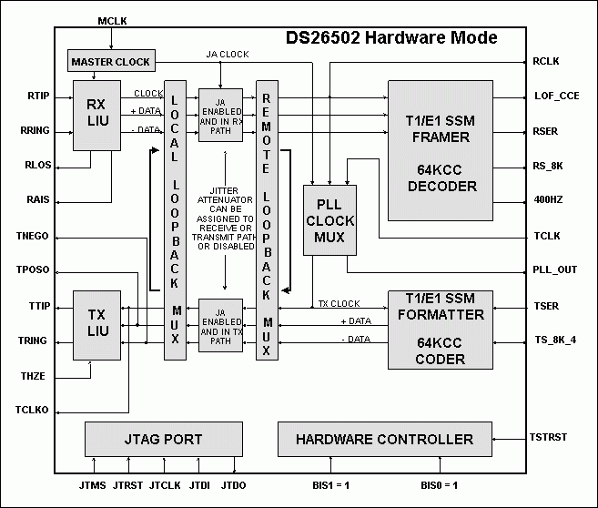
図1. DS26502のハードウェアモードのブロック図
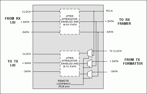
図2. ループバックの多重化ダイアグラム
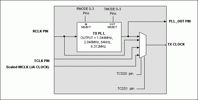
図3. 送信PLLクロックの多重化ダイアグラム
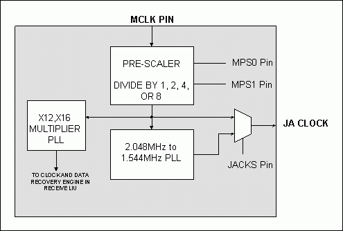
図4. マスタクロックPLLのダイアグラム
DS26502の概要
マキシムの通信製品の詳細については、T/Eキャリアおよびパケット化通信にあるデータシートをご参照ください。
マキシムデバイスの動作に関するご質問は、テレコムアプリケーションサポートチームまでお問い合わせください。