
アプリケーション・ノート使用上の注意
本アプリケーションノートの英語以外の言語への翻訳はユーザの便宜のために提供されるものであり、リビジョンが古い場合があります。最新の内容については、必ず最新の英語版をご参照ください。
なお、日本語版のアプリケーションノートは基本的に「Rev.0」(リビジョン0)で作成されています。

AN-1602: ADuM4135 ゲート・ドライバをMicrosemi APTGT75A120T1G 1200 V IGBT モジュールで使用する
はじめに
絶縁型ゲート・バイポーラ・トランジスタ(IGBT)は、オンボード・チャージャ、オフボード・チャージャ、DC/DC高速チャージャ、スイッチ・モード電源(SMPS)アプリケーションなどの高電圧アプリケーション向けの費用対効果の高いソリューションです。スイッチング周波数範囲はDC~100kHzです。IGBTは、単一デバイスとすることも、図1に示す設計のようにハーフ・ブリッジ・デバイスとすることも可能です。

このアプリケーション・ノートの設計で使用しているAPTGT75A120 IGBTは、Microsemi Corporation®独自のフィールド・ストップIGBTテクノロジを採用した高速トレンチ・デバイスです。また、このIGBTデバイスは、テール電流が低く、スイッチング周波数が最大20kHzで、対称設計のため浮遊インダクタンスが小さいソフト・リカバリ並列ダイオードも備えています。このIGBTを選択して高度な統合を行うことにより、接合部―ケース間の熱抵抗が低く、高周波で最適な性能を得ることができます。
IGBTは、アナログ・デバイセズのゲート駆動手法によって駆動できます。ADuM4135ゲート・ドライバは、25Vを超える動作電圧(VDD-VSS間電圧)時に7A(代表値)のソースおよびシンク電流駆動能力を持つ1チャンネル・デバイスです。このデバイスの最小コモンモード過渡耐圧(CMTI)は100kV/μsで、最大35Vを供給します。したがって、このアプリケーションには、±15V電源が適切です。
試験のセットアップ
電気的構成
システム試験回路の電気的構成を図2に示します。DC電圧がフル・ハーフ・ブリッジの両端の入力に印加されます。入力段には900μF(C1)のデカップリング・コンデンサが付加されています。出力段は、200μH(L1)と50μF(C2)のインダクタ・コンデンサ(LC)フィルタ段で、2Ω~30Ωの負荷(R1)への出力をフィルタ処理します。試験構成の電力部品を表1に示します。U1はHV+とHV−用のDC電源で、T1とT2は単一のIGBTモジュールです。

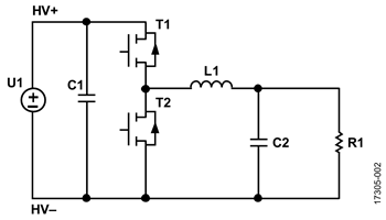
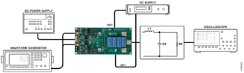
完成した電気的構成を図3に示します。試験で使用する機器のリストを表2に示します。
| Equipment | Value |
| IGBT Module, T1, T2 | APTGT75A120T1G1 |
| U1 | 200 V to 900 V |
| Capacitor C1 | 900 μF |
| Inductor L1 | 200 μH |
| Capacitor C2 | 50 μF |
| Load Resistor R1 | 2 Ω to 30 Ω |
| Equipment | Manufacturer | Part Number |
| Oscilloscope | Agilent | DSO-X 3024A, 200 MHz |
| DC Supply | Delta Elektronika | SN660-AR-11 (two in serial) |
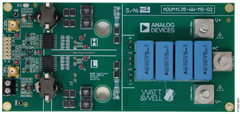
| Gate Driver Board | WATT&WELL | ADUM4135-WW-MS-02 SN001 |
| Waveform Generator | Agilent | 33522A |
| Current Probe | Hioki | 3275 |
| Current Probe | Hioki | 3276 |
| Passive Voltage Probe | Keysight | N2873A, 500 MHz |
| Passive High Voltage Probe | Elditest | GE3421, 100 MHz |
| High Voltage Differential Probe | Tektronix | P5200 |
| High Voltage Differential Probe | Testec | TT-SI 9110 |
| Thermal Camera | Optris | PI 160 |

テスト結果
無負荷試験
無負荷試験構成では、モジュールの出力に低出力電流が流れます。このアプリケーションでは、30Ωの抵抗を使用しています。
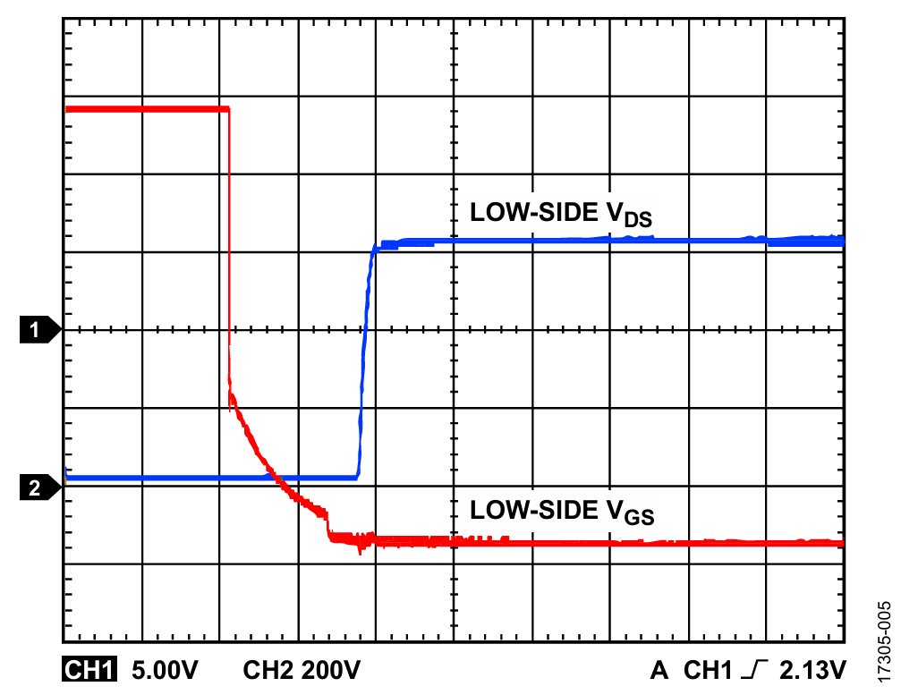
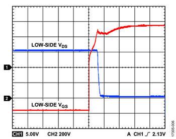
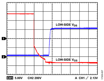
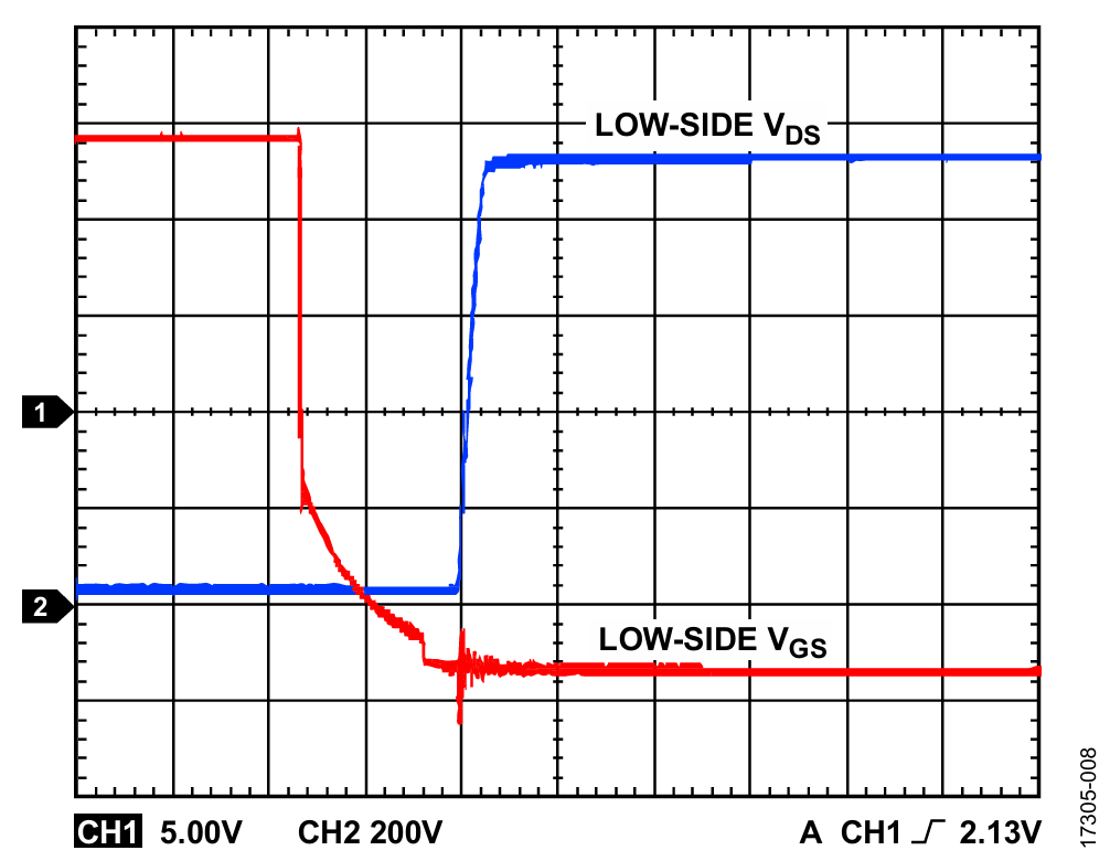
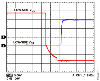
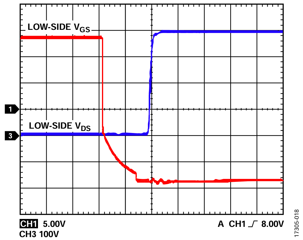
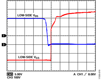
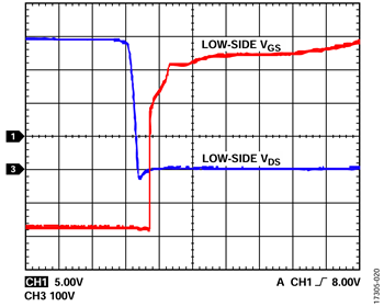
無負荷時の電気的試験構成の重要な要素と、負荷内のわずかな電流値を表3に示します。モジュールで観察された温度を表4に示します。表3と表4には、実測された結果をまとめています。様々な電圧とスイッチング周波数におけるスイッチング波形の試験結果を図5~図10に示します。
表3に示すように、試験1および試験2は600Vで実施しています。試験1は10kHzのスイッチング周波数で実施し、試験2は20kHzのスイッチング周波数で実施しています。試験3は、10kHzのスイッチング周波数にて900Vで実施しています。
無負荷試験の電気的構成を図4に示します。

| Test | DC Voltage, VDC1, (V) | Switching Frequency, fSW, (kHz) | Duty Cycle (%) | IIN2 (A) | Reference Figures |
| 1 | 600 | 10 | 50 | 0.007 | Figure 5 and Figure 6 |
| 2 | 600 | 20 | 50 | 0.013 | Figure 7 and Figure 8 |
| 3 | 900 | 10 | 50 | 0.009 | Figure 9 and Figure 10 |
1 VDCはHV+とHV−の電圧。
2 IINはU1を流れる入力電流。
| Test | VDC (V) | fSW (kHz) | Temperature | DC-to-DC Power Supply Temperature | Gate Driver Temperature | |||
| Ambient (°C) | Heat Sink (°C) | High-Side (°C)2 | Low-Side (°C)2 | High-Side (°C) | Low-Side (°C) | |||
| 1 | 600 | 10 | 26 | 30.8 | 34 | 34 | 38.2 | 37.6 |
| 2 | 600 | 20 | 26 | 31 | 35 | 35 | 39.5 | 39.4 |
| 3 | 900 | 10 | 26 | 31 | 34.2 | 34.2 | 38.6 | 37.7 |
1 すべての温度はサーマル・カメラで記録しています。
2 トランスで測定。
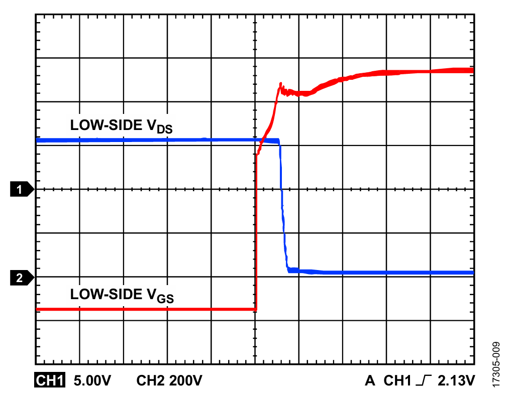
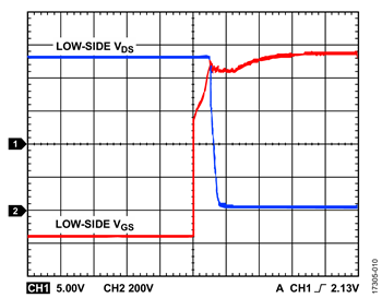
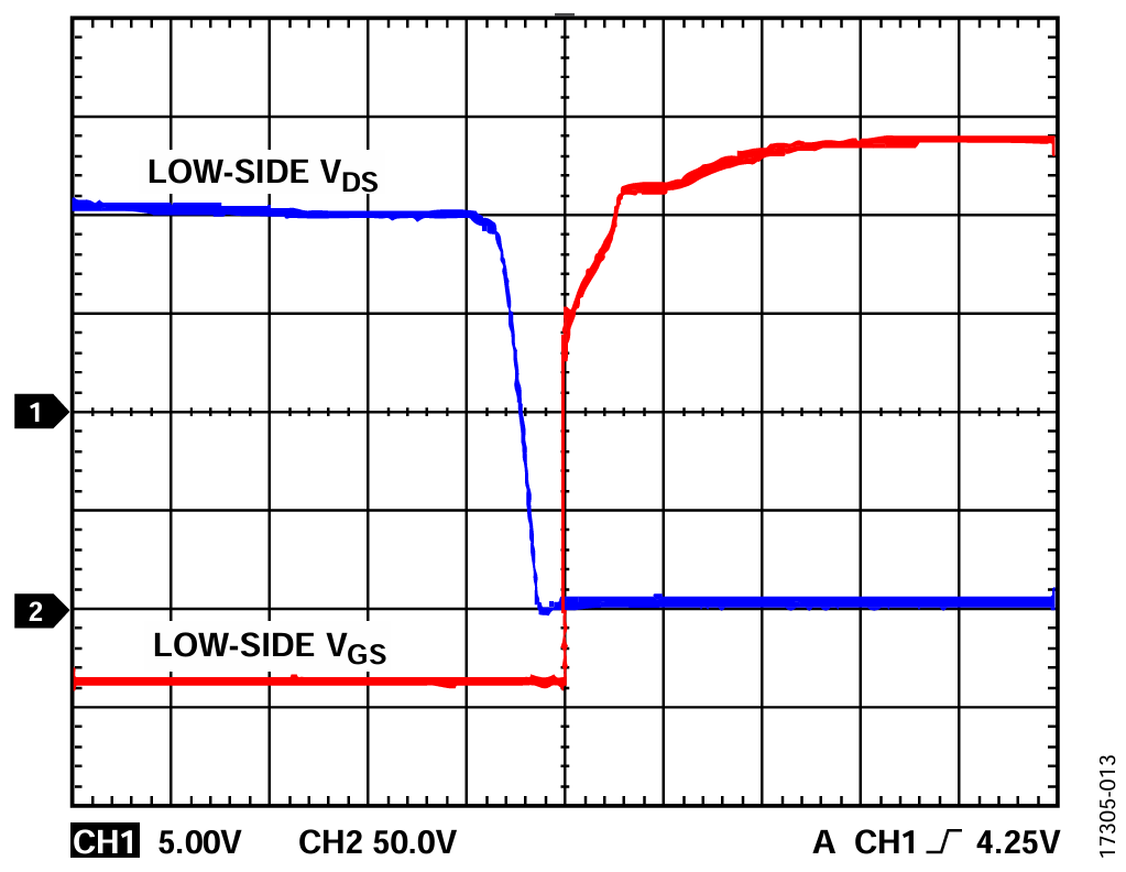
IGBTをオン/オフしたときの性能グラフ
このセクションの試験結果は、fSW = 10kHzおよび20kHzの場合の各種電圧でのスイッチング波形を示しています。VDSはVDRAINソースで、VGSはVGATEソースです。


負荷試験
試験構成は、無負荷試験のセクションにおける無負荷試験の試験構成(図4を参照)と似ています。実測結果を表5にまとめ、様々な電圧、周波数、負荷に対する試験から得られた性能と結果を図11~図16に示します。
試験4は、25%のデューティ・サイクルで、10kHzのスイッチング周波数にて200Vで実施しています。試験5は、25%のデューティ・サイクルで、10kHzのスイッチング周波数にて600Vで実施しています。試験6は、25%のデューティ・サイクルで、10kHzのスイッチング周波数にて900Vで実施しています。
| Test | VDC (V) | fSW (kHz) | Duty Cycle (%) | IOUT1 (A) | VOUT2 (V) | POUT3 (W) | IIN (A) | Reference Figures |
| 4 | 200 | 10 | 25 | 1.8 | 49.3 | 90.2 | 0.55 | Figure 11 and Figure 13 |
| 5 | 600 | 10 | 25 | 5.4 | 146.5 | 791.1 | 1.62 | Figure 12 and Figure 14 |
| 6 | 900 | 10 | 25 | 7.8 | 214 | 1669.2 | 2.5 | Figure 15 and Figure 16 |
1 IOUTは負荷抵抗R1の出力電流。
2 VOUTはR1に印加される出力電圧。
3 POUTは出力電力(IOUT × VOUT)。
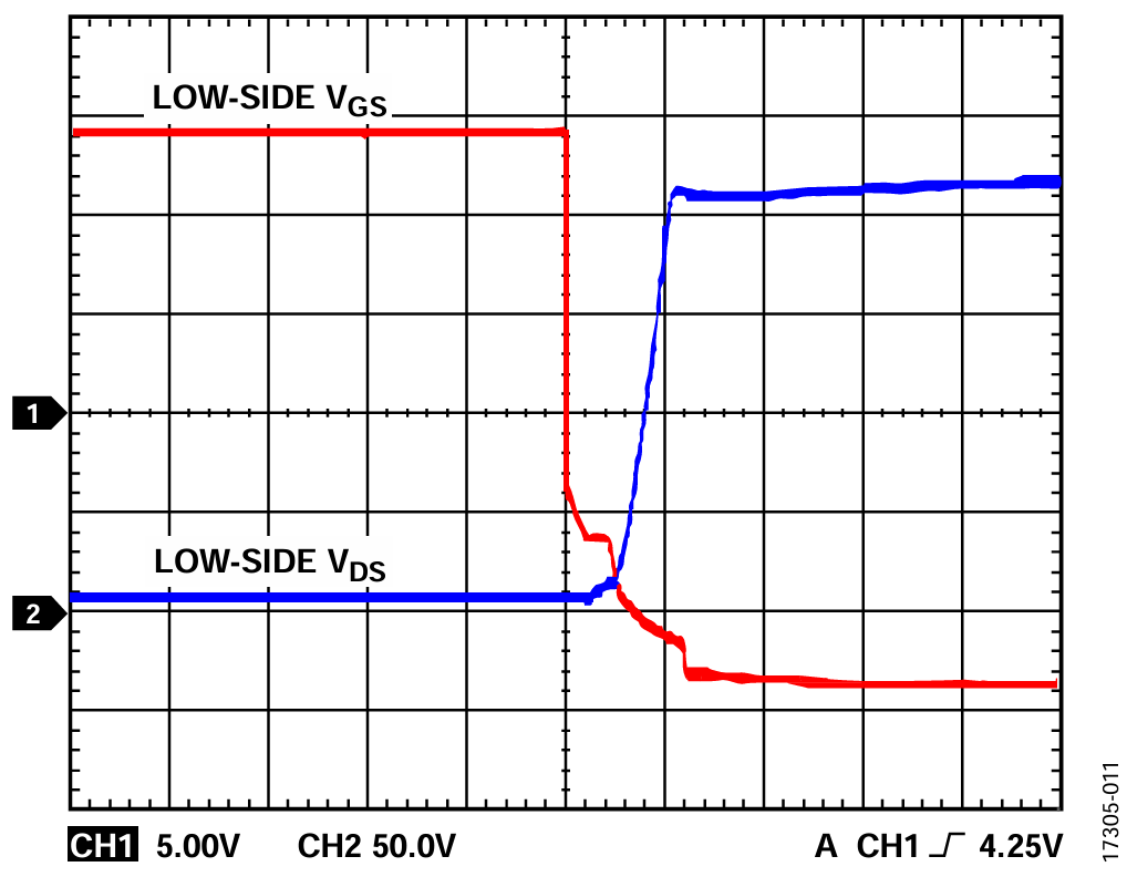
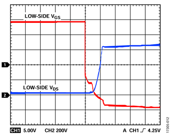
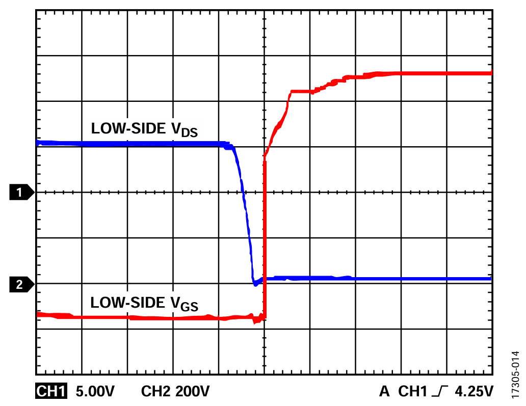
負荷試験でIGBTをオン/オフしたときの性能グラフ
このセクションの試験結果は、fSW = 10kHzおよび20kHzの場合の各種電圧でのスイッチング波形を示しています。


高電流試験
試験構成は図3に示した具体的な構成と似ています。実測結果を表6にまとめ、様々な電圧、周波数、負荷に対する試験から得られた性能と結果を図17~図20に示します。
出力負荷抵抗は試験ごとに異なります。表1に示すように、2Ωと30Ωの負荷を使って電流を変化させています。VOUTはR1の両端の電圧を測定したものです。
試験7は、25%のデューティ・サイクルで、10kHzのスイッチング周波数にて300Vで実施しています。試験8は、25%のデューティ・サイクルで、10kHzのスイッチング周波数にて400Vで実施しています。
| Test | VDC (V) | fSW (kHz) | Duty Cycle (%) | IOUT (A) | VOUT (V) | PIN1 (W) | IIN (A) | Reference Figures |
| 7 | 300 | 10 | 25 | 19.6 | 68.7 | 1346.3 | 5 | Figure 17 and Figure 19 |
| 8 | 400 | 10 | 25 | 25.8 | 91.7 | 2365.9 | 6.6 | Figure 18 and Figure 20 |
1PINは入力電力(IIN × VIN)で、VINはDC電源です。
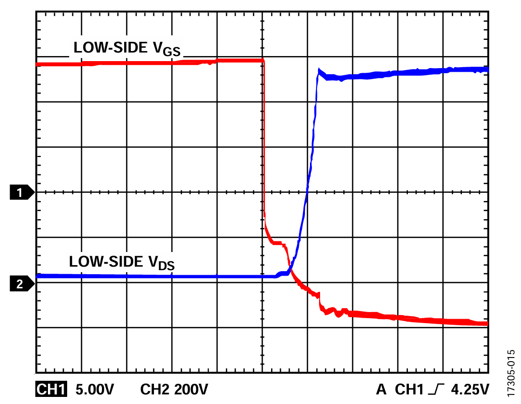
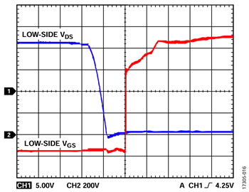
高電流試験でIGBTをオン/オフしたときの性能グラフ
このセクションの試験結果は、fSW = 10kHzおよび20kHzの場合の各種電圧でのスイッチング波形を示しています。


非飽和試験
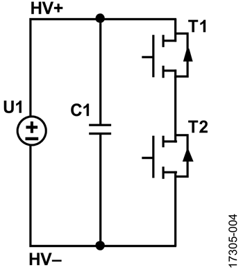
システム試験回路の電気的構成を図21に示します。DC電圧がフル・ハーフ・ブリッジ両端の入力に印加されます。入力段には900μFのデカップリング・コンデンサが付加されています。この設定は非飽和検出の試験に使用されます。このアプリケーションでは、最大IC = 150Aで、ICはT1とT2を流れる電流です。

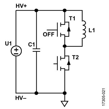
IGBTのハイサイド・スイッチ(T1)は83μHのインダクタでバイパスされており、T1スイッチはオフになっている必要があります。
IGBTのローサイド・スイッチ(T2)は500msごとに50μs間駆動されます。
非飽和試験構成のための電力部品の一覧を表7に示します。
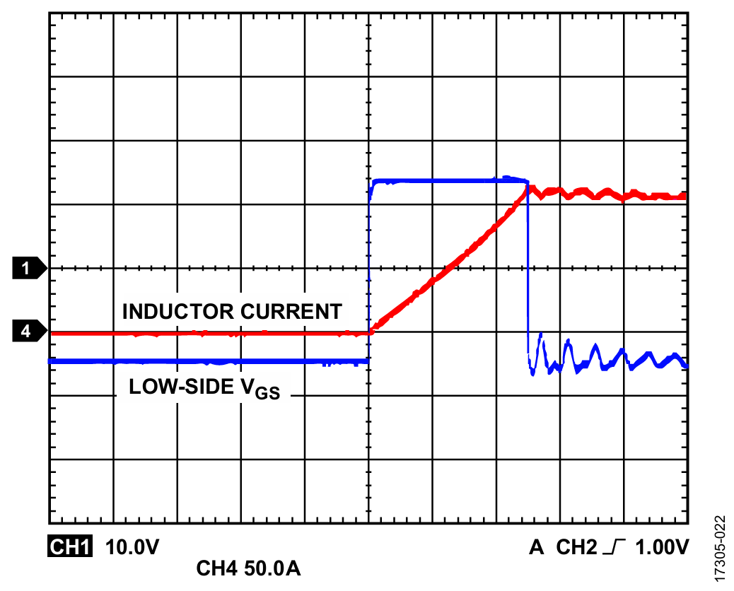
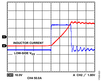
インダクタL1における135Aでのスイッチング・イベントを図22に示し、インダクタL1における139Aでの非飽和検出を図23に示します。
| Equipment | Value |
| U1 | 0 V to 80 V |
| C1 | 900μF |
| L1 | 83 μH |


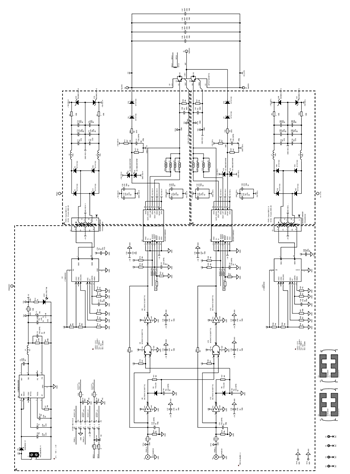
アプリケーション回路図

まとめ
ADuM4135ゲート・ドライバは電流駆動能力、適切な電源範囲、100kV/μsの強力なCMTI能力を備え、IGBTの駆動に最適な性能を発揮します。
このアプリケーション・ノートの試験結果は、ADuM4135評価用ボードが、IGBT駆動の高電圧アプリケーション向けソリューションであることを実証するデータを提供するものです。
著者
