Designed, Built, Tested
Board pictured here has been fully assembled and tested.

Overview

説明

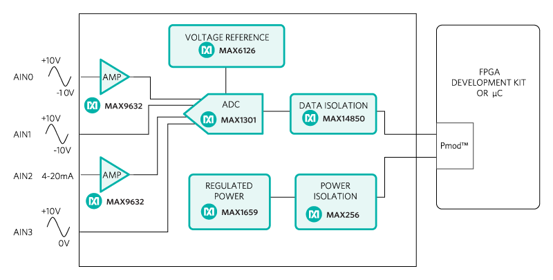
アナログ-デジタルコンバータ(ADC)を内蔵した最近のFPGA (field programmable gate array)およびマイクロコントローラは、低分解能で低電圧のアナログ入力に対応します。しかし、産業用制御および産業用オートメーションアプリケーションの必要を満たすには不十分であり、多くの場合、絶縁型の、より高分解能で、より高電圧のシステムソリューションが必要になります。Santa Fe (MAXREFDES5)サブシステムリファレンスデザインは、-10V~+10V、0~10V、および4~20mAの電流ループ信号を許容する16ビット高精度産業用アナログフロントエンド(AFE)で、絶縁された電源とデータを小型基板に集約しています。Santa Feデザインは、ローノイズハイインピーダンスアナログバッファ(MAX9632)、革新的なアッテネータを内蔵した高精度ADC (MAX1301)、超高精度4.096V電圧リファレンス(MAX6126)、600VRMSデータアイソレーション(MAX14850)、および絶縁型/安定化+12V、-12V、および5V電源レール(MAX256/MAX1659)を統合しています。このAFEソリューションは、高精度アナログ-デジタル変換を必要とするあらゆるアプリケーションで使用することができますが、主として産業用センサー、産業用オートメーション、プロセス制御、プログラマブルロジックコントローラ(PLC)、および医療アプリケーションを対象としています。

機能と利点

アプリケーション

  • 高精度
  • ±10V、0~10V、および4~20mA入力
  • 絶縁された電源とデータ
  • 小型のプリント基板(PCB)
  • デバイスドライバ
  • Cのソースコード例
  • Pmod™対応形状
  • 産業用センサー
  • プロセス制御
  • 産業用オートメーション
  • PLC
  • 医療

Details Section

図1. Santa Feサブシステムリファレンスデザインのブロック図

図1. Santa Feサブシステムリファレンスデザインのブロック図

必要機器:

  • 2つのUSBポートを備えたWindows® PC
  • Santa Fe (MAXREFDES5)ボード
  • Santa Fe対応プラットフォーム(すなわち、Nexys 3の開発キットまたはZedBoardキット)
  • 産業用センサーまたは信号源

適切なSanta Fe Quick Start Guideをダウンロードして読み、記載されている各ステップに注意深く従ってください。

Figure 1. Non-page mode memory interface.

Pmod仕様は、3.3Vと5Vの両方のモジュールおよびさまざまなピン割当てに対応します。このモジュールは3.3Vの電源電圧専用に設計されており、右の図に示すSPIピン割当てを使用しています。

電源要件を表1に示します。現在サポートされているプラットフォームおよびポートを表2に示します。

表1. Santa Feサブシステムリファレンスデザインの電源オプション
Power Type Jumper Shunt Input Voltage (V) Input Current (mA, typ)
On-board isolated power JU3: 1-2
JU4: 2-3
JU5: 1-2
3.3 221
External power JU3: 2-3
JU4: 1-2
JU5: 2-3
3.3 6.3
+12 30.4
-12 7.3
 表2. サポート対象プラットフォームおよびポート
Supported Platforms Port
Nexys 3 Platform (Spartan®-6) JB1
ZedBoard platform (Zynq®-7020) JA1
MicroZed platform (Zynq®-7010) J5

Santa Feのハードウェア設計は、特に-10V~+10V、0~10V、および4~20mAの信号を使用するアプリケーション向けに最適化されています。アプリケーションの要件に応じて、回路の特定の部分を省略することができます。どの部分が必要または省略可能かについては、このあとで詳しく解説します。「すべての設計ファイル」の項に記載された回路図のファイルを参照してください。

MAX1301 (U3)は、最大+12.288V~-12.288Vの入力電圧信号を許容可能な独自のマルチレンジ入力を備えた16ビット、逐次比較型(SAR) ADCです。また、このADCは入力抵抗17kΩのアナログ入力バッファを内蔵しています。

第1のアンプのMAX9632 (U1)は、ローノイズ、-10V~+10V入力電圧用に最適化されています。第2のアンプのMAX9632 (U2)は、ローノイズ、4~20mA入力電流用に最適化されています。U1およびU2の両方が、ソース抵抗の大きい入力信号、または4~20mAループの場合、250Ωの負荷抵抗に対して、高い入力インピーダンスを提供します。ソース抵抗が大きいと、多くの場合、望ましくない倍率で信号が減衰します。Santa Feデザインが給電されていないときに入力保護が必要な場合は、両方のMAX9632アンプの前にオプションの500Ωの直列抵抗を追加してください。500Ωの直列抵抗は、10Vが入力に印加されSanta Feボードが給電されていない場合に入力電流が最大入力電流仕様を超えるのを防ぎます。

信号源のソース抵抗が17kΩより大幅に低いか、または4~20mAループの場合、250Ωと17kΩの並列の組み合わせによってアプリケーションで許容可能な精度が得られる場合は、U1およびU2を除去することができます。ADCチャネルAIN1およびAIN3は、内蔵17kΩアナログ入力バッファのみを使用している例です。

ADCのMAX1301は4.096Vの電圧リファレンスを内蔵していますが、最高の精度を実現するには、0.02%の初期精度と3ppm/℃の最大温度係数(tempco)を備えた外付けの電圧リファレンスのMAX6126 (U4)を使用してください。

MAX256 (U5)は、3.3Vを入力として、1次側と2次側の巻数比が1:2.6の既製品のTGM-H281NF Halo®トランスおよびボード上の外付け電圧ダブラ回路を使用してそれを±12Vに変換する、絶縁型の、機能的絶縁クラスの電源ソリューションを提供します。ポストレギュレーションは低ドロップアウト(LDO)レギュレータのMAX1659を使用して実現されます。±12Vの絶縁型電源ソリューションはオプションで、アンプのMAX9632が高い入力インピーダンスを提供することが必要なアプリケーションまたは電源の絶縁が要求される場合にのみ必要です。アンプのMAX9632が不要の場合は、+6Vの絶縁型単一電源で回路全体に給電することができます。データの絶縁もアプリケーションに応じたオプションで、デジタルデータアイソレータのMAX14850 (U9)を使用して実現されます。電源とデータの組み合わせで実現される絶縁は600VRMSです。

Santa Feのファームウェア設計は、最初はNexys 3の開発キット用に発表され、Xilinx® Spartan-6 FPGA内に実装されたMicroBlaze™ソフトコアマイクロコントローラを対象としていました。現在サポートされているプラットフォームおよびポートを表2に示します。

ファームウェアは、ハードウェアへのインタフェース方法、サンプルの取得方法、およびサンプルのメモリへの保存方法を示す、実際に動作する例です。簡単なプロセスフローを図2aに示します。ファームウェアは、オープンソース規格のEclipse™に基づくXilinx SDKツールを使用してC言語で記述されています。標準Xilinx XSpiコアのバージョン3.03aを利用してSanta Fe固有の独自設計機能が作成されました。SPIクロック周波数は3.125MHzに設定されています。

Figure 2a. The Santa Fe firmware flowchart for Nexys 3 platform

図2a. Santa Feファームウェアのフローチャート(Nexys 3プラットフォームの場合)

ファームウェアは、コマンドの受信、ステータスの書込み、およびサンプリングしたデータブロックを仮想COMポート経由で標準端末プログラムにダウンロードすることが可能です。お客様の開発を迅速化するために、完全なソースコードが提供されています。コードの説明は、対応するファームウェアプラットフォームファイルに記載されています。

Santa Feファームウェア設計はZedBoard/MicroZedキットをサポートします。Xilinx Zynqシステムオンチップ(SoC)内のハードコアARM® Cortex®-A9プロセッサを対象としています。

ファームウェアは、ハードウェアへのインタフェース方法、サンプルの取得方法、およびサンプルのメモリへの保存方法を示す、実際に動作する例です。簡単なプロセスフローを図2bに示します。ファームウェアは、オープンソース規格のEclipseに基づくXilinx SDKツールを使用してC言語で記述されています。最大サンプリングレートを90kspsに高めるために、標準AXI Xilinx XSpiコアの代わりにARMの内蔵SPIペリフェラルを利用してSanta Fe固有の独自設計機能が作成されました。SPIクロック周波数は3.57MHzに設定されています。

図2b. Santa Feファームウェアのフローチャート(ZedBoardプラットフォームの場合)

図2b. Santa Feファームウェアのフローチャート(ZedBoardプラットフォームの場合)

ファームウェアは、コマンドの受信し、ステータスの書込みを行うと共に、仮想COMポートを経由してサンプリングしたデータブロックを標準端末プログラムにダウンロードすることが可能です。お客様の開発を迅速化するために、完全なソースコードが提供されています。コードの説明は、対応するファームウェアプラットフォームファイルに記載されています。

使用した機器:

  • 信号源のAudio Precision® SYS-2722または同等品
  • 2つのUSBポートを備えたWindows PC
  • Santa Fe (MAXREFDES5)ボード
  • Nexys 3の開発キット
  • +12V電源(外部電源での試験にのみ使用)
  • -12V電源(外部電源での試験にのみ使用)

Santa Feデザインを試験するときは、特別な注意を払い、適切な機器を使用する必要があります。あらゆる高精度設計の試験で重要なのは、試験対象の設計よりも高精度の信号源および測定機器を使用することです。以下に示す結果を再現するには、低歪みの信号源が絶対に必要です。入力信号は、Audio Precision SYS-2722を使用して生成されました。 アナログ入力は必ず信号源で駆動し、フローティングのままにしないでください。FFTは、Mitov Software社のSignalLabに含まれているFFTコントロールを使用して作成されました。表3は、図3~18に示すボード上の絶縁型電源と外部電源の両方についての各チャネルのACおよびDC性能のクイックリファレンスです。すべての実験室での測定結果は室温で測定したものです。

表3. 図3~18のAC性能(FFT)またはDC性能(ヒストグラム)のクイックリファレンスガイド
Channel Power Type Input Type Test Type Figure Number
Channel 0 (AIN0) On-Board Isolated ±10V, High AC - FFT Figure 3
Channel 0 (AIN0) On-Board Isolated ±10V, High DC - Histogram Figure 4
Channel 0 (AIN0) External ±10V, High AC - FFT Figure 5
Channel 0 (AIN0) External ±10V, High DC - Histogram Figure 6
Channel 1 (AIN1) On-Board Isolated ±10V, 17kΩ AC - FFT Figure 7
Channel 1 (AIN1) On-Board Isolated ±10V, 17kΩ DC - Histogram Figure 8
Channel 1 (AIN1) External ±10V, 17kΩ AC - FFT Figure 9
Channel 1 (AIN1) External ±10V, 17kΩ DC - Histogram Figure 10
Channel 2 (AIN2) On-Board Isolated 4–20mA, 250Ω AC - FFT Figure 11
Channel 2 (AIN2) On-Board Isolated 4–20mA, 250Ω DC - Histogram Figure 12
Channel 2 (AIN2) External 4–20mA, 250Ω AC - FFT Figure 13
Channel 2 (AIN2) External 4–20mA, 250Ω DC - Histogram Figure 14
Channel 3 (AIN3) On-board Isolated 0 to 10V, 17kΩ AC- FFT Figure 15
Channel 3 (AIN3) On-Board Isolated 0 to 10V, 17kΩ DC - Histogram Figure 16
Channel 3 (AIN3) External 0 to 10V, 17kΩ AC - FFT Figure 17
Channel 3 (AIN3) External 0 to 10V, 17kΩ DC - Histogram Figure 18


図3. ボード上の絶縁型電源、±10V 1kHzの正弦波入力信号、ハイインピーダンス入力、20kspsのサンプルレート、およびBlackman-Harris窓を使用したチャネル0 (AIN0)のAC FFT

図3. ボード上の絶縁型電源、±10V 1kHzの正弦波入力信号、ハイインピーダンス入力、20kspsのサンプルレート、およびBlackman-Harris窓を使用したチャネル0 (AIN0)のAC FFT


図4. ボード上の絶縁型電源、0Vの入力信号、ハイインピーダンス入力、20kspsのサンプルレートを使用したチャネル0 (AIN0)のDCヒストグラム、65,536サンプルで、コードの97.57%が中央の3 LSBに含まれる7 LSBのコード分布、および0.693の標準偏差

図4. ボード上の絶縁型電源、0Vの入力信号、ハイインピーダンス入力、20kspsのサンプルレートを使用したチャネル0 (AIN0)のDCヒストグラム、65,536サンプルで、コードの97.57%が中央の3 LSBに含まれる7 LSBのコード分布、および0.693の標準偏差


図5. 外部電源、±10V 1kHzの正弦波入力信号、ハイインピーダンス入力、20kspsのサンプルレート、およびBlackman-Harris窓を使用したチャネル0 (AIN0)のAC FFT

図5. 外部電源、±10V 1kHzの正弦波入力信号、ハイインピーダンス入力、20kspsのサンプルレート、およびBlackman-Harris窓を使用したチャネル0 (AIN0)のAC FFT


図6. 外部電源、0Vの入力信号、ハイインピーダンス入力、20kspsのサンプルレートを使用したチャネル0 (AIN0)のDCヒストグラム、65,536サンプルで、コードの97.74%が中央の3 LSBに含まれる7 LSBのコード分布、および0.692の標準偏差

図6. 外部電源、0Vの入力信号、ハイインピーダンス入力、20kspsのサンプルレートを使用したチャネル0 (AIN0)のDCヒストグラム、65,536サンプルで、コードの97.74%が中央の3 LSBに含まれる7 LSBのコード分布、および0.692の標準偏差


Figure 7. AC FFT for channel 1 (AIN1) using on-board isolated power, a ±10V 1kHz sine wave input signal, 17kΩ input impedance, a 20ksps sample rate, and a Blackman-Harris window.

Figure 7. AC FFT for channel 1 (AIN1) using on-board isolated power, a ±10V 1kHz sine wave input signal, 17kΩ input impedance, a 20ksps sample rate, and a Blackman-Harris window.


Figure 8. DC histogram for channel 1 (AIN1) using on-board isolated power; a 0V input signal; 17kΩ input impedance; a 20ksps sample rate; 65,536 samples; a code spread of 7 LSBs with 96.95% of the codes falling within the three center LSBs; and a standard deviation of 0.695

Figure 8. DC histogram for channel 1 (AIN1) using on-board isolated power; a 0V input signal; 17kΩ input impedance; a 20ksps sample rate; 65,536 samples; a code spread of 7 LSBs with 96.95% of the codes falling within the three center LSBs; and a standard deviation of 0.695


Figure 9. AC FFT for channel 1 (AIN1) using external power, a ±10V 1kHz sine wave input signal, 17kΩ input impedance, a 20ksps sample rate, and a Blackman-Harris window

Figure 9. AC FFT for channel 1 (AIN1) using external power, a ±10V 1kHz sine wave input signal, 17kΩ input impedance, a 20ksps sample rate, and a Blackman-Harris window


Figure 10. DC histogram for channel 1 (AIN1) using external power; a 0V input signal; 17kΩ input impedance; a 20ksps sample rate; 65,536 samples; a code spread of 7 LSBs with 97.70% of the codes falling within the three center LSBs; and a standard deviation of 0.691

Figure 10. DC histogram for channel 1 (AIN1) using external power; a 0V input signal; 17kΩ input impedance; a 20ksps sample rate; 65,536 samples; a code spread of 7 LSBs with 97.70% of the codes falling within the three center LSBs; and a standard deviation of 0.691


Figure 11. AC FFT for channel 2 (AIN2) using on-board isolated power, a 1V to 5V 1kHz sine wave input signal, high-impedance input, a 20ksps sample rate, and a Blackman-Harris window.

Figure 11. AC FFT for channel 2 (AIN2) using on-board isolated power, a 1V to 5V 1kHz sine wave input signal, high-impedance input, a 20ksps sample rate, and a Blackman-Harris window.


Figure 12. DC histogram for channel 2 (AIN2) using on-board isolated power; a 3V input signal; high-impedance input; a 20ksps sample rate; 65,536 samples; a code spread of 14 LSBs with 95.26% of the codes falling within the six center LSBs; and a standard deviation of 1.515

Figure 12. DC histogram for channel 2 (AIN2) using on-board isolated power; a 3V input signal; high-impedance input; a 20ksps sample rate; 65,536 samples; a code spread of 14 LSBs with 95.26% of the codes falling within the six center LSBs; and a standard deviation of 1.515


Figure 13. AC FFT for channel 2 (AIN2) using external power, a 1V to 5V 1kHz sine wave input signal, high-impedance input, a 20ksps sample rate, and a Blackman-Harris window

Figure 13. AC FFT for channel 2 (AIN2) using external power, a 1V to 5V 1kHz sine wave input signal, high-impedance input, a 20ksps sample rate, and a Blackman-Harris window


Figure 14. DC histogram for channel 2 (AIN2) using external power; a 3V input signal; highimpedance input; a 20ksps sample rate; 65,536 samples; a code spread of 14 LSBs with 95.52% of the codes falling within the six center LSBs; and a standard deviation of 1.506

Figure 14. DC histogram for channel 2 (AIN2) using external power; a 3V input signal; high-impedance input; a 20ksps sample rate; 65,536 samples; a code spread of 14 LSBs with 95.52% of the codes falling within the six center LSBs; and a standard deviation of 1.506


Figure 15. AC FFT for channel 3 (AIN3) using on-board isolated power, a 0V to10V 1kHz sine wave input signal, 17kΩ input impedance, a 20ksps sample rate, and a Blackman-Harris window.

Figure 15. AC FFT for channel 3 (AIN3) using on-board isolated power, a 0V to10V 1kHz sine wave input signal, 17kΩ input impedance, a 20ksps sample rate, and a Blackman-Harris window


Figure 16. DC histogram for channel 3 (AIN3) using on-board isolated power; a 5V input signal; 17kΩ input impedance; a 20ksps sample rate; 65,536 samples; a code spread of 8 LSBs with 96.07% of the codes falling within the four center LSBs; and a standard deviation of 1.006.

Figure 16. DC histogram for channel 3 (AIN3) using on-board isolated power; a 5V input signal; 17kΩ input impedance; a 20ksps sample rate; 65,536 samples; a code spread of 8 LSBs with 96.07% of the codes falling within the four center LSBs; and a standard deviation of 1.006


Figure 17. AC FFT for channel 3 (AIN3) using external power, a 0 to10V 1kHz sine wave input signal, 17kΩ input impedance, a 20ksps sample rate, and a Blackman-Harris window

Figure 17. AC FFT for channel 3 (AIN3) using external power, a 0 to10V 1kHz sine wave input signal, 17kΩ input impedance, a 20ksps sample rate, and a Blackman-Harris window


Figure 18. DC histogram for channel 3 (AIN3) using external power; a 5V input signal; 17kΩ input impedance; a 20ksps sample rate; 65,536 samples; a code spread of 10 LSBs with 96.77% of the codes falling within the four largest LSBs; and a standard deviation of 0.961

Figure 18. DC histogram for channel 3 (AIN3) using external power; a 5V input signal; 17kΩ input impedance; a 20ksps sample rate; 65,536 samples; a code spread of 10 LSBs with 96.77% of the codes falling within the four largest LSBs; and a standard deviation of 0.961

ツールおよびシミュレーション

ソフトウェア開発

Support & Training

Search our knowledge base for answers to your technical questions. Our dedicated team of Applications Engineers are also available to answer your technical questions.