Abstract
The combination of high switching frequency and high-voltage capability is difficult to achieve in IC design. You can, however, design an automotive power supply that operates with high frequency if you protect it from temporary high-voltage conditions. High-frequency operation is becoming important as more and more electronic functions are integrated into the modern automobile. This article discusses several ways to protect low-voltage electronic circuits from the harsh effects of the automotive electrical environment. Also included are the results of laboratory tests for noise immunity.
Introduction
The increasing density of electronics in automobiles presents unique challenges and opportunities to the power-system designer. Most automotive modules require low voltages such as 5V or 3.3V, but the use of linear voltage regulators to step down the battery voltage dissipates considerable power. Excessive power dissipation makes thermal management difficult and expensive. As a result, the increasing power requirements of faster processors and ASICs have steered the preferred method of power conversion from simple, low-cost, but inefficient linear regulation to the more complex but efficient switching converter.
Advantages of a Switching Converter
Passive components such as the power inductor and power capacitor can be physically smaller at higher switching frequencies, so the size of a switching converter depends on the switching frequency. By reducing power dissipation, high-efficiency converters also eliminate bulky and expensive heat sinks. Thus, the use of switching converters can shrink the overall size of the power supply. These advantages make the switching converter an increasingly attractive choice for power management in automotive applications such as body electronics, infotainment systems, and engine-control modules.
Considerations for Choosing a Switching Converter
The choice of switching frequency is critical, because a switching converter poses its own set of problems. The electromagnetic noise generated by its fundamental switching frequency and higher harmonics can interfere with other electronics. AM radio receivers, for example, are sensitive to interference in the range 530kHz to 1710kHz. A switching frequency greater than 1710kHz, therefore, eliminates fundamental and harmonic interference from the AM frequency band. Test data will show that the moderate voltage, high-frequency processes used with a simple protector, as in Maxim devices, are excellent solutions for addressing automotive power management needs. Ultimately, it is quite clear that designers no longer need high-voltage controllers to design these switching converters.
High-frequency switching also increases the power loss, which partly offsets the advantage of using a switching converter. Because switching losses are proportional to the operating voltage squared, they are worse at higher input voltages. Unfortunately, the typical automotive power-controller IC demands a high-voltage process (40V or higher) to withstand load dumps and other overvoltage transients. High-voltage processes incorporate larger geometries, thicker gates, and longer channel lengths, which produce longer propagation delays. These inherently slow processes become inefficient as well, because longer rise/fall times in the switch cause higher transition losses.
The advanced processes available to Maxim designers are suitable for extremely high-speed converters operating at moderate voltage levels. A dual-output 2.2MHz buck-boost converter (MAX5073), for example, can withstand inputs up to 23V. The converter's out-of-phase operation enables it to achieve an effective switching frequency of 4.4MHz.
Considering that switching converters are supposed to be immune to interference from the power source, you might ask, "Do automotive applications really need ICs with high-voltage capability?" The following discussion answers this question by describing the disturbances common to automotive power systems, and ways to protect low-voltage electronic systems from those disturbances.
Power-Line Overvoltage Stress Conditions
Overvoltage-protection (OV) devices isolate and protect electronic circuitry from excessive voltages conducted by electrical connections to the automotive electrical system, particularly those connections to the main voltage supply. The ability to withstand conducted disturbances is known as conducted immunity.
Automotive manufacturers and standards organizations specify various test methods for evaluating the conducted immunity of electronic components and systems. While automotive OEMs tend to have specific requirements, most of these specifications derive from the ISO7637 standard. The following is a brief summary of the typical OV conditions relevant to automotive applications. This summary is not intended to be a comprehensive description of all conducted immunity requirements.
Steady-State OV Conditions
Certain OV conditions are of sufficiently long duration to be considered steady-state from the standpoint of an electronic circuit. An example is any OV condition that persists longer than the thermal time constant of an associated electronic device. In these situations, the continuous power dissipation and resulting temperature rise are a primary concern. Steady-state conditions include a failed alternator regulator, a "double-battery jump start," and reversed-battery connections. The following is a brief description of each.
Failed Alternator Regulator. An alternator's output is adjusted for speed, load, and temperature by regulating the magnitude of current in the field winding. That adjustment is usually provided by an electronic circuit (a voltage regulator), which ensures a constant, regulated alternator output by pulse-width modulating (PWM) the alternator's field winding. A typical set point for the voltage regulator's output is 13.5V. However, the voltage regulator can fail in a way that applies the full field current, regardless of load or output-voltage conditions.
When that failure happens, the entire system can be subject to voltages beyond the typical 13.5V. (Actual voltage levels depend on vehicle speed, loading, and other conditions.) A typical OEM test requirement for failed regulators is 18V for one hour. Most systems are required to withstand the stress of that test, although certain comfort and convenience functions are allowed to deviate from normal operation.
Double-Battery Jump Start. Another steady-state OV condition is the double-battery jump start, which occurs when a tow truck or other service personnel use 24V to jump-start a disabled vehicle or otherwise charge a dead battery. The typical OEM test requirement for this condition is about 24V for two minutes. Some systems related to safety and engine management are required to operate under these conditions.
Reverse Battery Conditions. A steady-state reverse potential can be inadvertently applied to a vehicle's electrical system during manufacturing or service. For that condition, most systems are required to survive but not operate. The typical requirement is -14V for one minute. That test can be a challenge for systems that require high current or a low-voltage drop.
Transient OV conditions
In an automobile the majority of transient OV conditions are caused by switching inductive loads. Such loads include the starter motor, fuel pump, window motors, relay coils, solenoids, ignition components, and distributed circuit inductances. Interrupting the current in any of these inductive loads produces a OV pulse. Filters, metal-oxide varistors (MOVs), or transient-voltage suppressors are used to suppress such OV transients, according to the amplitudes and durations involved. Figures 1 through 4 illustrate the suppression requirements based on the ISO7637 standard. Table 1 is a representative summary of actual OEM requirements, which are largely based on the ISO7637 standard.

Figure 1. In response to repetitive switching action, this circuit produces repetitive negative pulses with amplitudes from -80V to -150V and durations from 1ms to 140ms. A typical source impedance is 5Ω to 25Ω.

Figure 2. In response to repetitive switching action, this circuit produces positive repetitive pulses with amplitudes from +75V to +150V, and a typical duration of 50µs. A typical source impedance is 2Ω to 10Ω.

Figure 3. Repetitive switching action in the circuits shown produces a series of -150V, 100ns negative pulses (Pulse 3a), and a series of 100V, 100ns positive pulses (Pulse 3b). The source impedance is typically 50Ω.

Figure 4. A load-dump pulse occurs when an alternator is suddenly disconnected while delivering high current to a discharged battery. The sudden reduction in current induces high voltage at the alternator output to maintain the energy in the system. The duration of this transient depends on the electrical time constant of the alternator field circuit and the regulator response time.
| Pulse Type | OEM#1 | OEM#2 | OEM#3 | OEM#4 | OEM#5 | OEM#6 | OEM#7 | OEM#8 | |
| Pulse 1 | Td | 2ms | 2ms | 2ms | 2ms | 5ms | 50µs | 140ms | 46ms |
| Vp | -100V | -100V | -100V | -150V | -100V | -100V | -80V | -80V | |
| Rs | 10Ω | 10Ω | 10Ω | 10Ω | 25Ω | 10Ω | 5Ω | 20Ω | |
| Pulse 2 | Td | 50µs | 50µs | 50µs | 50µs | 2ms | 5.7µs | ||
| Vp | 150V | 50V | 100V | 75V | 200V | 110V | |||
| Rs | 4Ω | 2Ω | 10Ω | 2Ω | 10Ω | 0.24Ω | |||
| Pulse 3a | Td | 100ns | 100ns | 100ns | 100ns | 100ns | 4.6ms | ||
| Vp | -150V | -150V | -150V | -112V | -150V | -260V | |||
| Rs | 50Ω | 50Ω | 50Ω | 50Ω | 50Ω | 34Ω | |||
| Pulse 3b | Td | 100ns | 100ns | 100ns | 100ns | 100ns | |||
| Vp | 100V | 100V | 100V | 75V | 100V | ||||
| Rs | 50Ω | 50Ω | 50Ω | 50Ω | 50Ω | ||||
| Pulse 5 | Td | 300ms | 400ms | 300ms | 120ms | 500ms | 380ms | ||
| Vp | 50V | 100V | 43.5V | 80V | 70V | 60V | |||
| Rs | 0.5Ω | 2Ω | 0.5Ω | 2.5Ω | 0.5Ω | 0.75Ω | |||
| *The voltages and durations are for the guidance only. Actual numbers may vary. | |||||||||
As mentioned earlier, battery voltage cannot be fed directly to the low-voltage, high-performance switching converters. Instead, the battery is frequently connected by a transient-voltage suppressor such as a MOV, or a bypass capacitor followed by a traditional input-voltage limiter. These simple circuits are built around the p-channel MOSFET (Figure 5a). The p-channel MOSFET must be rated at 50V or 100V, depending on the expected level of voltage transients expected at the VBAT input.
A 12V zener diode (Z1) prevents the MOSFET gate-to-source voltage from exceeding VGSMAX. The MOSFET operates in saturation when the input voltage (VBAT) is below the breakdown voltage of zener Z2. During an input-voltage transient, the MOSFET blocks voltages higher than the Z2 breakdown voltage. The disadvantage of this approach is that it requires an expensive p-channel MOSFET and the numerous components associated with it.
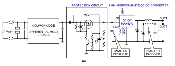
Figure 5a. The pass element in this input voltage-limiting circuit (protection circuit) is a p-channel MOSFET.
Another approach uses an NPN transistor. The NPN base voltage is clamped to VZ3, which regulates the emitter voltage at (VZ3 - VBE). This solution is inexpensive, but the VBE drop incurs a power loss: PLOSS = IIN × VBE. The VBE drop also increases the critical parameter of minimum-required battery voltage, especially during cold-crank operations (Figure 5b). A third option uses an n-channel MOSFET. The n-channel MOSFET is widely available, less expensive, and useable as a blocking element. Its gate drive is complicated, however, by the need for VG to go higher than the source voltage.

Figure 5b. The pass element in this input voltage-limiting circuit (protection circuit) is an NPN transistor.

Figure 5c.The pass element in this input voltage-limiting circuit (protection circuit) is an n-channel MOSFET.
The block diagram of Figure 5c shows the use of an n-channel MOSFET switch as a blocking device. During a load dump, the MOSFET turns off completely when VBAT increases above the set limit. The MOSFET then remains off for as long as VBAT remains above the set voltage. An overvoltage-protection controller (MAX6398) protects the high-performance power supply from automotive overvoltages (like load dumps and double-battery voltage) by controlling the n-channel MOSFET. Figure 6 diagrams this approach. The following Figures 7 through 9 show the results of the noise immunity testing done in the lab and the practical implementation of a transient protector using an n-channel MOSFET.

Figure 6. The MAX5073 2MHz buck converter is shown with the MAX6398 protection switch at the front-end. This design combines high performance and high-interference immunity.

Figure 7. Test results show switching waveforms and input ripple for the MAX5073 dual buck converter. The individual converter's switching frequency was 2.2MHz, while the input capacitor's ripple frequency was 4.4MHz. (CH1 = SOURCE2; CH2 = SOURCE1; CH3 = Input Capacitor Ripple; CH4 = CLKOUT.).

Figures 8A and 8B. Pulse 5 (80V, 120ms, OEM#5) was applied at the input of the protector. The MAX5073 is connected at the output of protector, and the converter's Output-1 and Output-2 are monitored.
These waveforms show the response at the protector output of Figure 6 and the two converter outputs, at 1s/cm (A) and 1ms/cm (B) (CH1 = VBAT; CH2 = VPROT; CH3 = Output-1; CH4 = Output-2.)

Figures 9A and 9B. Pulse 5 (70V, 500ms) was applied at the protector switch's input in Figure 6. The MAX5073 is connected at the output of protector, and the converter's Output-1 and Output-2 were monitored.
These waveforms show the response at the protector output and the two converter outputs, at 1s/cm (A) and 200µs/cm (B). ( CH1 = VBAT; CH2 = VPROT; CH3 = Output-1; CH4 = Output-2.)
As depicted in Figure 9, the MAX6398 effectively blocks automotive load-dump pulses and regulates the voltage seen by low-voltage, high-performance electronics. The strategy of using a combination of protector and low-voltage, high-frequency electronics saves space and cost compared to the high-voltage solution operating at significantly lower frequency.
A similar article appeared in the December 2006 issue of Selezione.
Latest Media 21


