Digital Control Enables High Reliability DC-to-DC Power Conversion with Active Snubbing
Digital Control Enables High Reliability DC-to-DC Power Conversion with Active Snubbing
Sep 1 2016
Typically, for isolated dc-to-dc power supply applications with high output current, the use of synchronous rectifiers (particularly MOSFETs) is dominant. A high output current also introduces a high di/dt on the rectifiers. For high efficiency, the choice of MOSFET is mainly determined by the on resistance and the gate charge. However, little attention is given to the parasitic body diode reverse recovery charge (Qrr) and output capacitance (COSS). These are critical parameters that contribute to the voltage spike and the ringing seen on the drain of the MOSFET. Typically, as the break-down voltage rating of the MOSFET increases, the on resistance also increases. This article proposes a digitally controlled active clamp snubber that can eliminate the voltage spike and ringing seen on the synchronous rectifiers. It also offers a design guide coupled with several other benefits in isolated dc-to-dc converters (such as half- and full-bridge topologies), while improving reliability and reducing failure rate.
Introduction
High reliability power supplies with high meantime between failures (MTBF) are always desired. For a robust design, a higher breakdown voltage rating of the switches can be used. However, this leads to a loss of efficiency. As a result, high efficiency and high reliability are somewhat opposed in their application. There has been steady demand within the industry for high efficiency isolated dc-to-dc converters as part of next-generation power supply solutions. This requires the use of synchronous rectifiers for the secondary side. Rectifiers are generally rated from 1.2 to 1.5 times the voltage spike across the device. The voltage spike is caused by the resonance from the leakage inductance, parasitic trace inductance, and rectifier output capacitance (COSS), which can resonate up to a peak value of twice the steady state reverse voltage of the rectifier. Passive snubbers can be used in the form of RC1 or RCD2 as a solution. While these are popular, they are also lossy and contribute to a small drop in efficiency. Some techniques to generate a lossless snubber use regenerative snubbers like LCD3 focus on snubbers for the primary side switch only or use the RC snubber during power switch turn-off only and not during turn-on. Other techniques4, 5 use the leakage energy to drive a small high efficiency converter to feed into the output voltage terminal. However, this requires a higher component count. Other techniques6 have applied the active clamp snubber to the full-bridge, phase-shifted topology to eliminate resonance caused by the resonant inductor on the primary side in a ZVS soft switching application, which has a limitation at low duty cycles.
This article takes a closer look at the active clamp snubber circuit and its digital implementation, which can prevent a voltage excursion with special emphasis on eliminating reverse recovery losses of parasitic diodes in MOSFETs that provide several other added benefits. The schematic of the power stage of the converter (secondary side only) is shown in Figure 1.

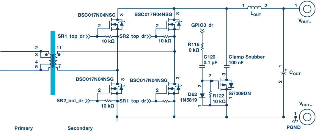
Figure 1. Secondary side of the power converter showing active clamp.
Figure 1 shows the secondary side of an isolated dc-to-dc converter. The secondary side consists of synchronous rectification in the form of an H-bridge connected to the transformer. Also present are the output filter inductor (LOUT) and output filter capacitor (COUT). The active clamp switch is a P-channel MOSFET and the gate drive for level shifting the gate signal consists of a capacitor and a diode.
High Frequency Equivalent Circuit
In the high frequency view, the large inductors and large capacitors are considered to be open circuited and short circuited, respectively, while only the parasitic and resonating inductances and capacitances are used for circuit analysis. This method allows the circuit to be simplified to analyze the ac currents. This is particularly useful in resonant topologies and where snubbers are involved because high frequency currents will choose the path of least impedance during the snubbing period.
The ac view of the circuit is shown in Figure 2. The output filter inductor and output filter capacitor are open circuited and shorted, respectively. Output capacitances of the MOSFETs and leakage inductances are left as they are in the circuit. Focus is on the secondary side of the converter, as the primary voltage source is shorted and does not contribute to the analysis.

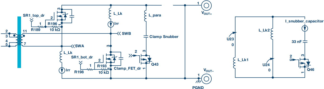
Figure 2. (Left) AC view of the secondary side of the power converter showing active clamp. (Right) simplified ac view.
Operation of the Active Clamp Circuit for the Synchronous FET
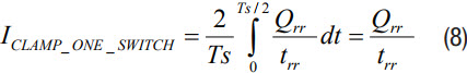
In the analysis, the snubber capacitor is assumed to be sufficiently large enough to maintain a constant voltage across it. During the freewheeling interval (SR1 and SR2 are both turned on in Figure 3), all of the four secondary switches (MOSFETs) are turned on. Due to finite rise and fall times, and variability in propagation delays of the gate drive signals, there is always a small dead time between the synchronous rectifier signals. During this dead time, the parasitic body diode of the MOSFETs conducts to enable freewheeling. Following this is the next half of the switching period where the other leg of the primary MOSFET is fired. This causes the polarity to change across the transformer winding and turn off the synchronous rectifier body diode. However, the parasitic diode of the synchronous MOSFET does not turn off as long as the reverse recovery charge (Qrr) isn’t depleted. The direction is shown in Figure 2. This Qrr is seen as an excess of current reflected through the transformer to the primary side as a leading edge spike. This also contributes to the voltage spike on the drain terminal of the synchronous MOSFET. The magnitude of the reverse recovery charge is given by:
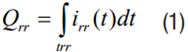

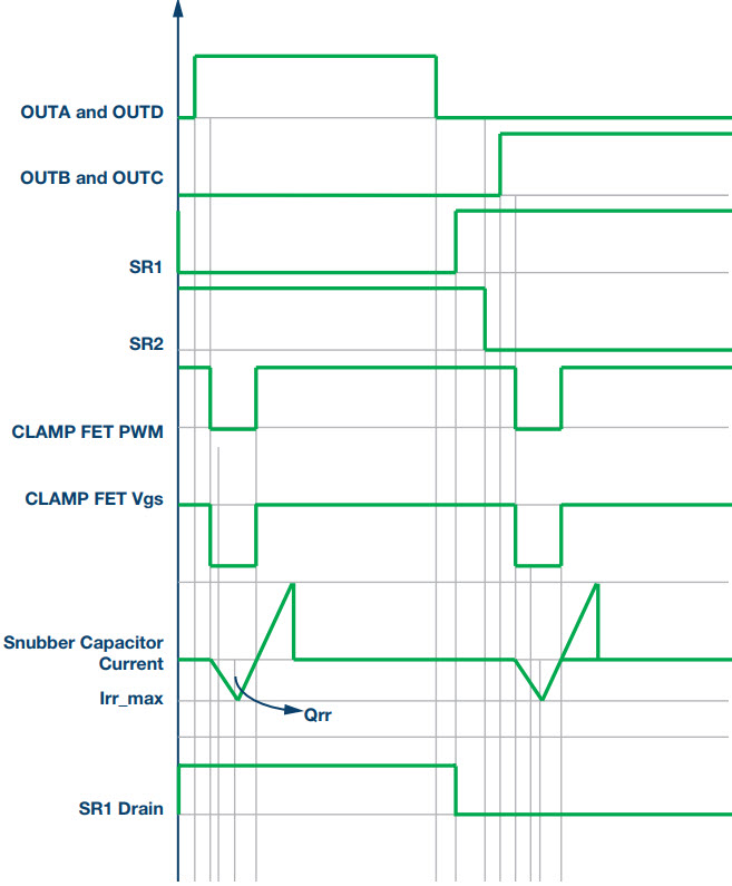
Figure 3.

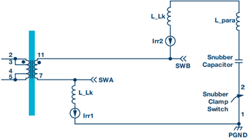
Figure 4a. Operation during trr interval capture of reverse recovery energy.

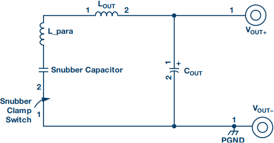
Figure 4b. Energy released in the load.
A voltage spike caused by the leakage and trace inductance (polarity shown in Figure 2) is absorbed by the active clamp snubber. The active snubber switch can be turned on at ZVS after the parasitic diode is turned on. However, when the active clamp snubber turns on, the snubber capacitor absorbs the reverse recovery current and recirculates the captured energy into the secondary bridge and the load. Since the net current through snubber capacitor is zero, it will maintain the charge balance as long as the converter operates in steady state.
Design Guideline
1. Estimation of Leakage Inductance
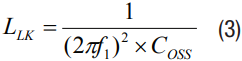
Operate the converter without the snubber and measure the resonant frequency and period (f1) of the ringing voltage spike on the drain of the synchronous MOSFET. Also, measure the leading edge spike on the primary current waveform (which should be equal to trr). To estimate the leakage inductance, place a known value of the capacitor (C2) at least one order of magnitude greater than the drain source capacitance of the MOSFET. Measure the ringing frequency (f2) and calculate the capacitance (COSS) and leakage (LLK) inductance using the equations below:
2. Selection of Active Clamp Snubber Capacitor
Choose a snubber capacitor with at least 10 to 100 times the output capacitance of the synchronous MOSFET. This is because there will be a low impedance path to the active snubber switch. However, the choice of the snubber capacitor must be such that:
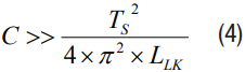
where Ts is the switching period.
Turn the active clamp snubber on with the small delay shown below:
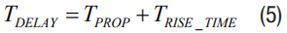
The two terms are the propagation delay of the driver and the driver signal rise time of the primary MOSFET. This timing is critical as the entire reverse recovery of the MOSFET body diode must be captured. This time depends on the reverse recovery characteristics of the body diode (Qrr, trr, Irr) of the synchronous MOSFET and can vary with factors across the device such as temperature, load current, and reverse voltage. The timing delay and snubber on time can be optimized for different characteristics of switches using fine resolution settings as described.
An alternate method of sizing the clamp capacitor is by using the following equation. It is based on the resonant period where the leakage energy is dumped into the clamp capacitor.
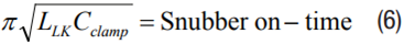
This value will range from:
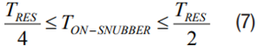
To avoid excessive ringing observed in Point 1, the on time should be up to one or two resonant periods or else there will be excessive and continuous ringing. Alternately, the on time of the snubber can be approximated to the on time of the leading edge spike observed in Point 1 above (such as trr). Excessive on time simply causes the energy to resonate for several more cycles, and this can be seen in the primary current waveform (Figure 8 and Figure 9).
3. Snubber Switch Selection
A simplified version of (1) is to take the worst-case limit from the data sheet of the MOSFET. The following equation provides more insight to the current in the capacitor:
The factor of 2 is used because only half a switching period is considered, and this process occurs twice for a full-bridge or half-bridge topology. Also in Figure 1, since two switches turn off, the reverse recovery charge is doubled. Hence, the total current is given by:

where C is 2 for full-bridge configuration; C is 1 for the center tapped transformer; and N is the number of MOSFETs in parallel. This is the average current through the active snubber switch.
Digital Implementation
The digital implementation of the active clamp snubber has two controls: Control 1 is the snubber delay (that is the adjustable delay in the snubber PWM edge from the trigger edge). Control 2 is the snubber PWM on time. The trigger point is the logical OR of the rising edge of the primary PWMs of the opposite legs of the H-bridge (for example, OUTC and OUTD). The snubber PWMs don’t require as high of a resolution as the main PWM resolution (for example, 125 ps). As a result, the clock required for triggering can be at a relatively slower speed (5 ns resolution), which also saves power (40× factor). The concept can also be applied to power conversion topologies that have a center tap on the secondary. In addition, the concept can be further applied to individual switches where a discrete active clamp-switch snubber cell is placed across each of the power transistors. In this case, the drive signals for the active clamp FETs are taken from the falling edge of the synchronous rectifiers.

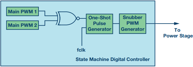
Figure 5. Digital implementation of snubber PWM.
The ADP1055 digital controller offers the right set of tools to accomplish this. With an intuitive GUI, the optimization of the active clamp snubber can be performed in a matter of minutes. The ADP1055 offers two options to set the snubber PWM using a logical combination of SR1 and SR2, or OUTC and OUTD signals. In both cases, the snubber PWM can be configured with two options as shown in Figure 6 and Figure 7. In all the above mentioned scenarios, the optimization parameters can be fine-tuned using the snubber delay (sets the dead time) and the snubber on time features. The logical combination of the two signals with polarity selection offers complete freedom for the user to select the right set of snubbers.

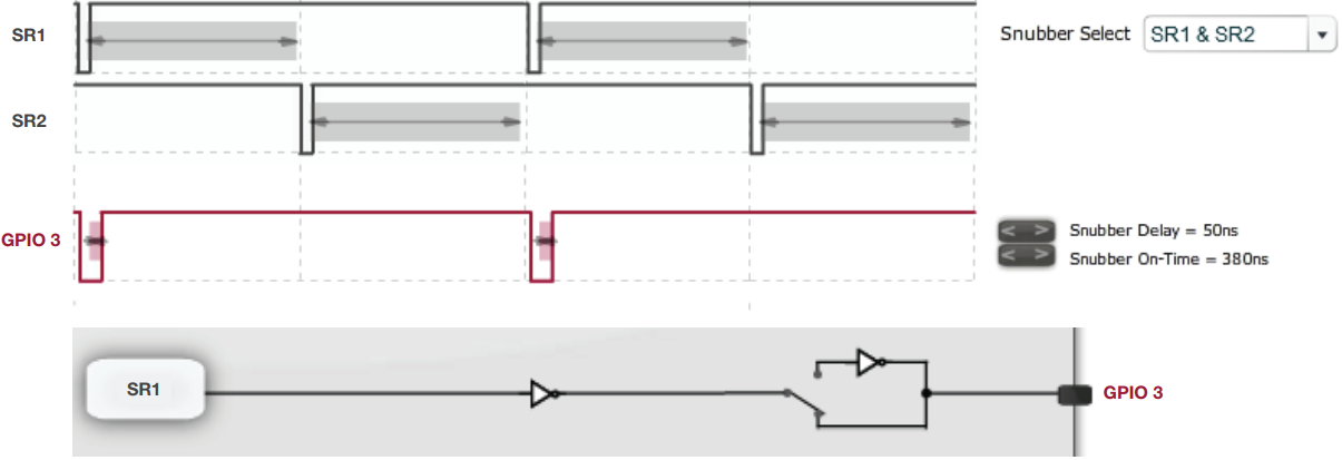
Figure 6. Snubber timings using Option 1—SR1 and SR2.

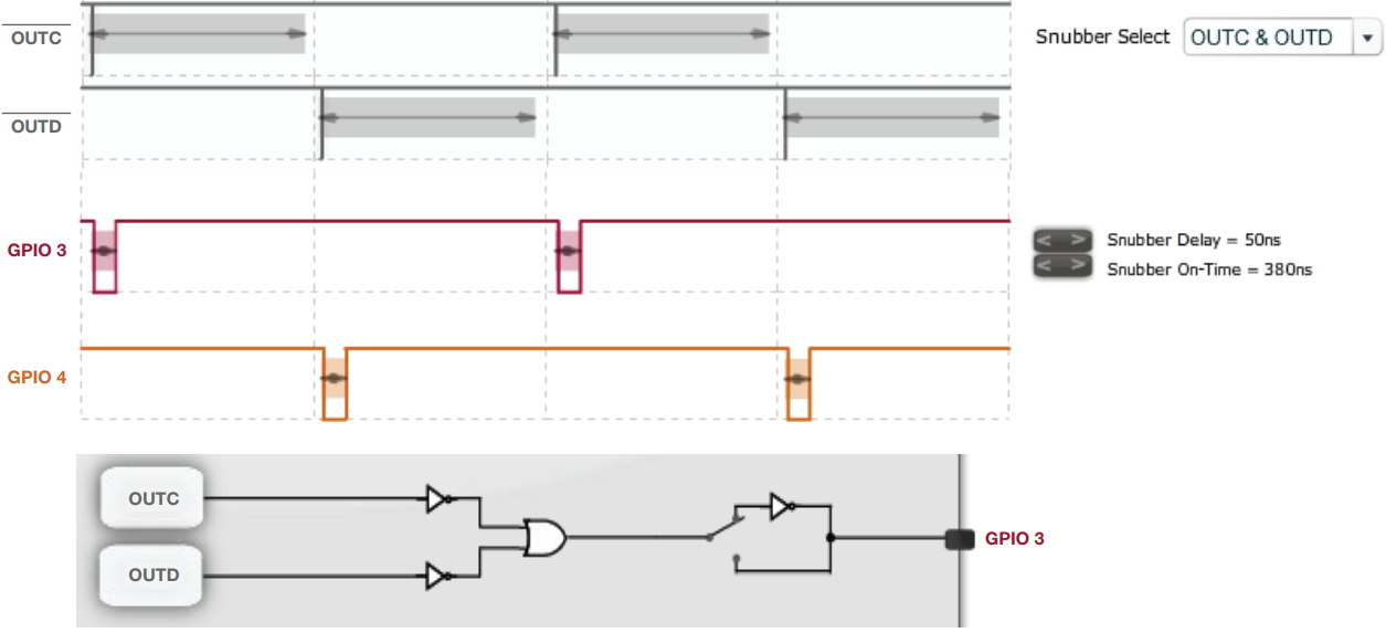
Figure 7. Snubber timings using Option 2—OUTC and OUTD.
Experimental Results on Full-Bridge Topology
For experimental verification, an isolated dc-to-dc converter was chosen with a nominal input of 48 V and an output rated at 12 V, 20 A at a switching frequency of 125 kHz. The topology is full-bridge with a secondary side as described in Figure 1.
Figure 8 shows how an incorrect snubber on time creates excessive ringing and the oscillation drain voltage of the synchronous MOSFET, which is also reflected in the primary current. The leading-edge spike is also severe and contributes to unwanted EMI.

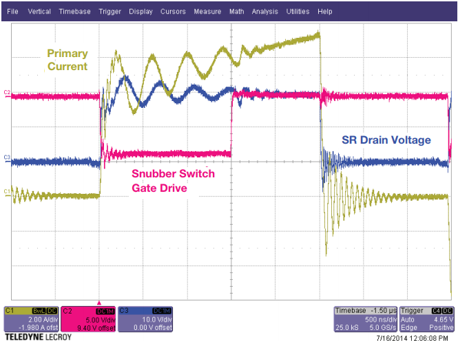
Figure 8. Excessive on time of the snubber.
Figure 9 shows an optimized snubber on time where there is no ringing on the drain voltage of the synchronous MOSFET. Also the leading-edge spike has been nearly eliminated.

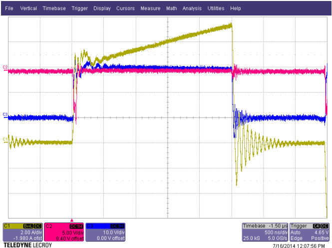
Figure 9. Optimized timing of the snubber.
Figure 10 shows the drain voltage of the synchronous MOSFET without the active clamp snubber. The voltage excursion can be as severe as 1.5 times the steady state voltage with the possibility of the MOSFET going into an avalanche condition.

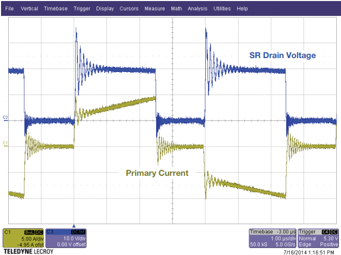
Figure 10. Without active clamp snubber.
Figure 11 shows the effectiveness of the active clamp snubber. The leading edge spike is completely eliminated and there is no ringing on the drain of the MOSFET.

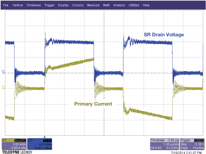
Figure 11. With active clamp snubber.

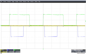
Figure 12. Snubber effectiveness at 0 A load.
Green trace: SR drain, 10 V/div
Blue trace: clamp FET gate-source voltage, 5 V/div
Yellow trace: load current, 10 A/div

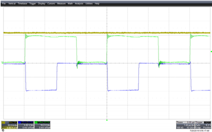
Figure 13. Snubber effectiveness at 20 A load.
Green trace: SR drain, 10 V/div
Blue trace: clamp FET gate-source voltage, 5 V/div
Yellow trace: load current, 10 A/div
Experimental Results on Half-Bridge Topology
Additional experimental verification was performed on a half-bridge topology with a nominal input of 48 V and an output rated at 9 V, 200 W at a switching frequency of 180 kHz.

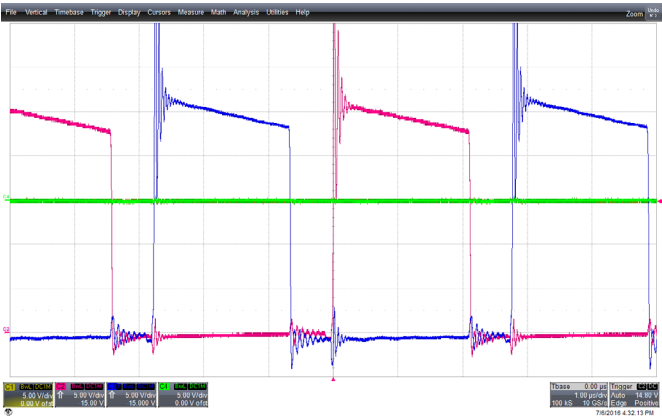
Figure 14. Active clamp snubber disabled.
Red trace: SR1 drain, 5 V/div
Blue trace: SR2 drain; 5 V/div
Green trace: snubber PWM, 5 V/div

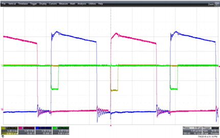
Figure 15. Active clamp snubber enabled.
Red trace: SR1 drain, 5 V/div
Blue trace: SR2 drain, 5 V/div
Green trace: snubber PWM, 5 V/div.

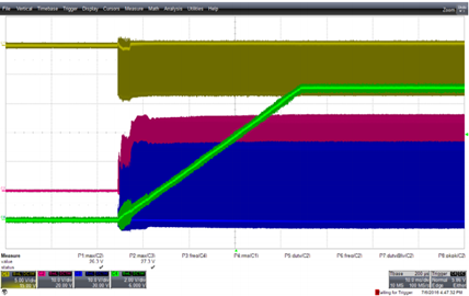

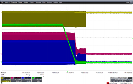
Figure 17. SR drain waveforms during soft start with active clamp snubber.
Yellow trace: snubber FET gate-source voltage, 5 V/div
Red trace: SR1 drain, 10 V/div
Blue trace: SR2 drain, 10 V/div
Green trace: output voltage, 2 V/div

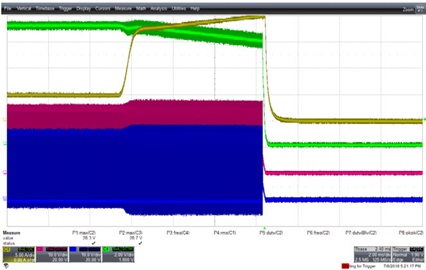
Figure 18. SR drain voltages during short-circuit test.
Yellow trace: load current, 5 A/div
Red trace: SR1 drain, 10 V/div
Blue trace: SR2 drain, 10 V/div
Green trace: output voltage, 2 V/div
Layout Considerations
Figure 8 shows a layout for the half-bridge topology mentioned above. The key takeaway is to reduce the parasitic inductance of the clamp loop by shortening or tightening the loop to a narrow area. Failure to do so will mitigate the effectiveness of the clamp, leading to high frequency rinsing during the clamp period.

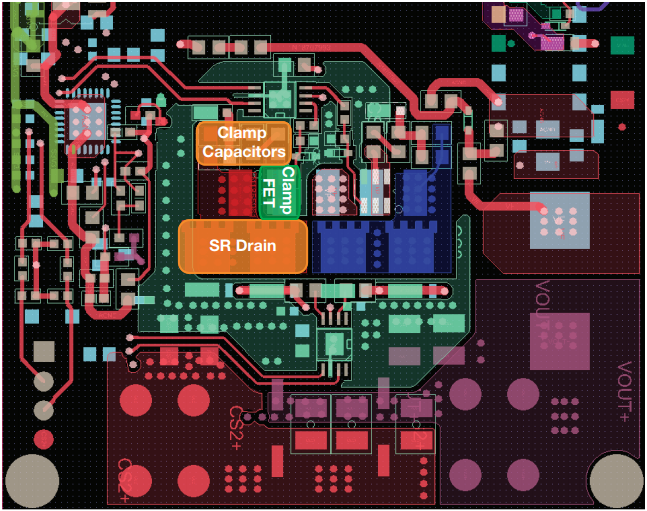
Figure 19. Layout for active clamp snubber.
Conclusion
This article has shown digital implementation of the active-clamp snubber circuit for high output current applications in isolated dc-to-dc converters. The proposed active-clamp scheme offers several benefits, such as lower clamping voltage that leads to a lower MOSFET breakdown voltage rating, leading to higher efficiency. It also eliminates ringing, which lowers electromagnetic interference (EMI). It is a low cost and simple circuit with an easy drive scheme. It also offers PCB board savings compared to other active snubbers involving additional inductors. Overall, the reliability of the power supply is dramatically increased. Furthermore, the leading-edge spike is eliminated, and this reduces the stress on the primary switches. Additionally, a higher efficiency translates to lower heat generation, which is useful for modules in a constrained area where it is difficult to dissipate heat.
The ADP1055 digital controller offers the right set of tools to accomplish the tasks mentioned above without the use of complex programming or coding. The ADP1055 also supports many other features, such as black-box, soft stop, command masking, and nonlinear gain.
About the Authors
Subodh Madiwale is a staff applications engineer in the Power Management Division of Analog Devices (San Jose). Previously, he held a position at Power Integrations as an FAE designing power supplies. His interests include...
Related to this Article
Products
{{modalTitle}}
{{modalDescription}}
{{dropdownTitle}}
- {{defaultSelectedText}} {{#each projectNames}}
- {{name}} {{/each}} {{#if newProjectText}}
-
 {{newProjectText}}
{{/if}}
{{newProjectText}}
{{/if}}
{{newProjectTitle}}
{{projectNameErrorText}}
Latest Media 21


