Abstract
Thanks to lackluster efficiency in currently available RF power amplifiers (PAs), the addition of wireless communications to hand-held computing devices entails unusual power-management techniques. Some communications protocols allow burst-transmission techniques and shutdown when not transmitting (duty-cycle control), but during a transmission the typical PA efficiency is no greater than 40% to 60%. In contrast, efficiency for the main power supply in a hand-held device is typically 90% to 95%.
Many hand-held devices operate from one to four nonrechargeable alkaline batteries. Others that demand the higher levels of instantaneous power associated with backlit displays achieve longer life (between charges or between battery replacements) with NiMH or even Li+ batteries. Regardless of battery type and configuration, however, the modem, PA, and radio circuitry necessary for wireless communications call for extra battery capacity if the system is to maintain a reasonable operating life.
Typical of such systems is a PCMCIA wireless modem for transferring cellular digital packet data (CDPD). It might plug into a hand-held personal digital assistant (PDA) or a hand-held computer running Windows® CE, drawing several hundred milliamps from a 3.3V supply. The PCMCIA card usually includes a secondary battery to avoid excessive drain on the host battery. To supply the power surge demanded during transmission, secondary batteries usually exhibit the low equivalent series resistance (ESR) found in today's popular rechargeable chemistries. Actual power for the wireless link depends primarily on the PA's transmitting power and efficiency.
As an example, the power supply (including the backup battery) for a wireless data-communications link must interface with a host hand-held system operating at 3.3V (Figure 1 - note the tiny packages appropriate to a hand-held system: IC1 in a 16-pin QSOP, and IC2 in an 8-pin µMAX®). The secondary battery is a single lithium-ion cell that exhibits a full-charge voltage of 4.1V to 4.2V and has little residual energy below 2.9V. IC1 converts this voltage to 3.3V, and IC2 forces the resulting backup voltage to track the host supply within 12mV (0.36%).
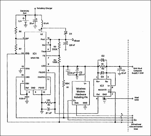
Figure 1. This circuit adds wireless-modem and power-amplifier capability to a hand-held instrument, along with appropriate power-management functions.
Tracking is crucial for the proper mating of the wireless hardware and the host. It ensures that the bidirectional data and control lines achieve valid logic levels, and it prevents excessive current flow from the primary battery to the modem hardware and from the secondary battery to the primary battery and the electronics.
The circuit operates as follows. First, consider the modem's state before it is plugged into the host's PCMCIA slot. None or very little energy should be drawn from the secondary battery, so the modem's power supply must be disabled for that condition. The on/off control line for this secondary supply is active-low PG of IC2. Because VHH from the host that powers IC2 is not present when the modem is disconnected, IC2 is powered down.
As its power good (active-low PG) output (an internal open-drain n-channel MOSFET) offers high impedance when the power is off, it draws only leakage current. While this active-low PG output is high-Z, the two resistive dividers (R6/R7, which normally monitors the secondary-battery voltage by means of a comparator internal to IC1, and R3/R4, which sets the VBOOST level when power is applied) shut down IC1 by acting as pullups on the active-low ONB line. IC1's switch-mode boost regulator and low-dropout (LDO) regulator are both disabled during shutdown. Thus, with 1µA leakage through the dividers and 1mA into IC1, the typical battery drain during shutdown is just 2µA.
Consider the power requirements when the supply voltage is applied: If the PA must produce 0.6W and is 50% efficient, it requires 1.2W of input power. If it operates with a 50% duty cycle (equal time for transmitting and receiving), then RMS power into the PA is 0.6W. At 3.3V supply voltage, this load draws about 180mA. If the rest of the modem draws 40mA from 3.3V, the total supply current for the wireless link is about 220mA¹ at 3.3V.
The IC1 boost regulator can deliver (at VBOOST) approximately 800mA from a 2.7V source and 1A or more from a virtually depleted Li+ cell (2.9V to 3.0V). Even so, the PA and the remaining modem hardware are powered by the less efficient internal LDO, which is rated 300mA typical with about 220mA as a guaranteed minimum. The reason is noise suppression. The LDO offers approximately 38dB of PSRR at 300kHz, giving it an advantage in suppressing the PWM switching noise at VBOOST. By easing or eliminating the need for subsequent noise suppression on the PA's supply voltage and associated RF emissions, this built-in filter action by the LDO makes it easier to pass the FCC emissions requirements. The efficiency hit, on the other hand, is approximately 8.3%.
VBOOST tracks VHH in the neighborhood of 3.3V. The secondary battery has a voltage higher than VBOOST when fully charged and lower than VBOOST when near depletion, so the LDO and boost regulator in tandem provide a necessary buck/boost function. SEPIC, flyback, and forward configurations can also achieve the buck/boost function, but they all require bulky and expensive magnetic storage elements (transformers) and lack the noise suppression provided by an LDO. In this regard, the circuit shown in Figure 1 is superior to all the alternatives.
Next, consider what happens when you plug the modem card into the host's PCMCIA connector. This action makes electrical connections between the respective circuit commons (GND) and between all bidirectional data and control lines. The host can then enable or disable the modem hardware using the EN line. If this line is initially low when the hardware is mated, then all the modem hardware is disabled and presents high impedance to the LDO node.
IC2 receives power when the host computer's VHH supply (nominally 3.3V) charges C1 through the connector, and IC2's minimum operating voltage allows a proper power-up even when VHH is at the low end of its range (10% below nominal). An internal 15µs delay allows VHH to settle (at the V+ terminal) before the active-low PG output goes low, notifying the host that the modem circuitry can now be enabled by the EN line. Low (virtual ground) on active-low PG also grounds the two resistor dividers for proper sensing of the battery and boost-regulation voltages.
When VHH is connected, IC2 pulls active-low ONB low when active-low PG goes low, and IC1 begins shuttling energy through L1, raising VBOOST (by means of feedback from R3/R4) to approximately 3.7V. Initially the LDO regulator is held off. It turns on when VBOOST achieves regulation, and IC1 enters its tracking mode when the LDO output is above 2.3V (it should be near 3.3V already, because VHH has charged C2 through R2). Tracking mode, a special feature of IC1 that forces VBOOST to 300mV above the LDO voltage, is set by the connection between OUT and TRACK. The 300mV headroom allows the LDO to maintain regulation while providing the required PSRR up to its maximum output-current rating. Because tracking mode automatically forces the boosted voltage to the minimum necessary, the LDO wastes minimum battery power.
The LDO is in regulation when IC1's FBLDO pin assumes the internal reference voltage (nominally 1.23V). This FBLDO voltage is generated by current through R5, which is proportional to the current through R2. That is, IC2 has the transfer function VOUT = gm(VSENSE)R5, where VOUT is the voltage across R5, VSENSE is the voltage across the RS+ and RS- terminals (R2), and gm = 10-2 mho. When in regulation, VOUT = VFBLDO = 1.23V. Therefore,
VSENSE = VFBLDO/(gm*R5).
Substituting for VSENSE in the relation VLDO = VHH + VSENSE,
VLDO = VHH + VFBLDO/(gm*R5).
Substituting numerical values from the circuit in Figure 1,
LDO = VHH + 1.23/(10-2*104) = VHH + 12.3mV.
Setting R5 to 10kΩ forces the sense voltage to 12.3mV. Knowing this, one can select R2 to program the amount of current flowing from LDO to VHH. At R2 = 1kΩ, for instance, this R2 current is approximately 12µA.
The intended use for IC2 (a high-side current-sense amplifier) is in precision measurements of high-side current using low-value high-wattage precision-current-sense resistors. This application is unusual in that 10%-accurate low-wattage current-sense resistors are fine (1/16W surface-mount types, for instance). We don't care exactly how much current flows from LDO to VHH. We just care that it remains small.
As one advantage of the high-value (1kΩ) current-sense resistor, a short circuit or an unexpected heavy load at VLDO can draw only 3.3mA or so through R2 from the host, which is hardly enough to cause a system crash. R2 needn't be as large as 1kΩ; IC2 draws about 800mA, so setting R2 = 12mV/800µA = 15W allows the LDO node (instead of the host) to power IC2.
In an alternate configuration, IC2's V+ node can be connected directly to LDO instead of VHH. IC2 then receives power from LDO, except at power-up, when the power comes from VHH through R2. This arrangement requires that the PA and the modem hardware be shut down, presenting a high impedance to LDO that forms no significant voltage division with R2, and that R2 be sufficiently small to ensure the minimum voltage allowed at V+ for guaranteed operation (3V). If VHH = 3.6V or more, for example, R2 must be less than 375Ω. This value ensures that IC2's 0.8mA operating current drops no more than 0.3V at the low end of the VHH range (3.6V - 10%).
The Schottky diodes (D2, D3) in parallel with R2 protect IC2 from excessive voltages between RS+ and RS-. They introduce small leakage currents but don't otherwise influence circuit behavior. The capacitor in parallel with R5 ensures a smooth and stable VLDO voltage by shunting high-frequency noise at the LDO feedback node to ground. As mentioned earlier, IC1 includes a comparator with uncommitted input and output. In this circuit it monitors the secondary battery voltage and alerts the host when the remaining energy is close to a level critical for maintaining the communications link.
Note that the circuit in Figure 1 accommodates a range of conditions beyond those described above. It is compatible with other communications buses suitable for mating a wireless modem to a hand-held device, for example. These include the cardbus and the strongly emerging universal serial bus (USB). This circuit also accepts host-supply voltages up to 5V nominal. For greater efficiency, some applications connect the PA directly to VBOOST instead of VLDO. In that case, VBOOST need not track VLDO; the voltages can be controlled separately with independent sets of feedback resistors.
IC1 starts at 1.1V and operates down to 0.7V, so even a two-cell NiMH secondary battery is acceptable for boost applications that require lower levels of RF output power. Finally, IC1 normally operates as a low-noise PWM regulator under a heavy load with a switching frequency of ~300kHz. If necessary, you can control this waveform's harmonic energy content by synchronizing its frequency (by means of the CLK/SEL line) to an external source in the 200kHz-to-400kHz range. For light load conditions in which the radiated and conducted energy is relatively low, you can force IC1 (again by means of the CLK/SEL line) into the pulse-frequency modulation (PFM) mode that provides the highest efficiency and the longest battery life.
¹ If the PA duty cycle is <100% and the LDO's output current is within the limits rated for IC1, use the equation i*t = C*V to size the LDO output capacitor (C2) such that any dips of LDO voltage during transmission are within allowable limits.
Related to this Article
Products
1 to 3 Cell, High Current, Low-Noise, Step-Up DC-DC Converters with Linear Regulator
Low-Cost, Precision, High-Side Current-Sense Amplifier
Product Categories
{{modalTitle}}
{{modalDescription}}
{{dropdownTitle}}
- {{defaultSelectedText}} {{#each projectNames}}
- {{name}} {{/each}} {{#if newProjectText}}
-
 {{newProjectText}}
{{/if}}
{{newProjectText}}
{{/if}}
{{newProjectTitle}}
{{projectNameErrorText}}
Latest Media 20


