Abstract
Powering white-LEDs in today's handheld electronics requires specialized regulators. Two common styles of regulators exist, each with its own advantages and disadvantages. This application note discusses the strengths of each type of regulator. The MAX1561 and MAX1573 are used as examples.
Today's handheld electronics commonly incorporate color LCD displays with white LEDs as the backlight. Optimally powering white LEDs requires specialized regulators that both overcome the high forward-voltage of the LED and provide constant-current drive to minimize intensity variations with battery voltage and between LEDs. For this purpose, there are two mainstream regulator types: inductor-based boost converters and capacitor-based charge-pump converters. Each regulator type has specific advantages/disadvantages, so optimal selection depends on the system's particular priorities.
This article compares a state-of-the-art regulator of each type, the MAX1561 boost converter versus the MAX1573 charge pump. The merits of each regulator type are evaluated, and the conclusions will aid system designers in selecting an appropriate solution. The MAX1561 and MAX1573 are especially well suited for comparison because both products were designed at the same time, are fabricated in the same facility on the same process, and both switch at the same 1MHz frequency.
Schematic Complexity: Slight Advantage to Charge Pump
Figure 1 shows the schematics for both regulator solutions. The circuits are simple with only a few external components, but the boost convert requires an inductor and Schottky diode. (Some competing boost converters integrate the Schottky diode, but usually with a reduction in efficiency.)

Figure 1. The MAX1561 boost converter (a) and MAX1573 charge pump (b) are two state-of-the-art alternatives for powering white LEDs. Circuit complexity is similar, but the charge pump does not require an inductor.
Efficiency: Surprising Slight Advantage to Charge Pump
Figure 2 shows the efficiency for both solutions. Efficiency was measured as the power in the LEDs divided by the battery power during a standardized Li Ion battery C/5 discharge profile. The curves at 18mA/LED represent efficiency at normal backlight brightness levels; the averages for both the boost converter and charge pump are 83%. Also shown are curves at 2mA/LED, representing the efficiency when dimmed during extended periods of inactivity; the charge pump obtains excellent 76% average efficiency compared to the boost converter's 59%.
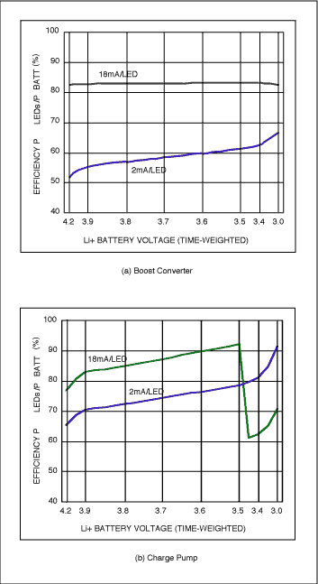
Figure 2. Both the MAX1561 boost converter (a) and MAX1573 charge pump (b) average 83% efficiency at 18mA/LED over the Li+ battery life. However, when dimmed at 2mA/LED, the charge pump is much more efficient than the boost converter.
The above results are somewhat surprising because most charge pumps are not nearly this efficient. The MAX1573 obtains its class-leading efficiency by including 1x pass-through and 1.5x boost charge-pump modes, adaptive mode switchover, and very low-dropout linear current regulators to stay in the more efficient 1x mode for as long as possible as while the battery declines. Older charge pumps without 1x mode typically obtain only 50% to 67% efficiency. Also, some competing charge pumps that do include a 1x mode, fail to use it for most of the battery life and, therefore, obtain far less than 83% average efficiency.
Turning to boost converters, the MAX1561 is one of the industry's most efficient. Nonetheless, higher efficiency is possible if a tradeoff is made. A good example is the MAX1599, which achieves 87% efficiency at 18mA/LED and 71% at 2mA/LED. The MAX1599 is exactly the same as the MAX1561, except that its oscillator is slowed from 1MHz to 500KHz to reduce switching losses. Due to the reduced frequency, the physical size of the inductor is doubled.
Physical Size: Advantage to Charge Pump
Figure 3 shows the PCB footprint for both solutions, including external components. While the boost converter's lower pin-count allows a smaller 3mm × 3mm package, the inductor results in a larger total footprint and greater height. Inductors approaching 1mm height will require even more board space than shown in Figure 3. Although the charge pump is in a larger 4mm × 4mm package, it only requires four small 1uF ceramic capacitors. Figure 3(b) shows the capacitors as 0603 size, but at least three manufacturers already offer them in smaller 0402 size, as shown in Figure 3(c). For extremely space-constrained applications, the MAX1573 charge pump is also available in a tiny 2mm × 2mm chip-scale package, making the entire charge pump solution possible in only 11mm2.
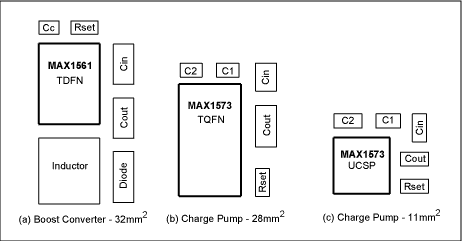
Figure 3. Due to the need for an inductor, boost converters (a) require more board area and height than do charge pumps (b). With chip-scale packaging and 1uF 0402 size capacitors, a charge pump solution (c) becomes extremely small.
System Flexibility: Advantage to Boost Converter
One important advantage for the boost converter is that the LEDs are connected in series, compared to the charge pump's parallel arrangement. As seen in Figure 4(a), this series configuration requires only two traces between the boost converter and the LEDs. This is especially an advantage if the LEDs are mounted in a separate display module, while the boost converter or charge pump remains on the main system PCB. In such a case, the boost converter consumes fewer connector terminals. Additionally, the same boost converter circuit may be utilized across a large number of models, each using a different number of LEDs in the display module. Or the display module in any particular model may be changed at any time with no impact on the boost converter circuit. Conversely, the boost converter may be changed with no impact on the display module. This LED series-connection significantly reduces risks to a design schedule.
To make a charge pump efficient, the 1x mode necessitates an individual current regulator for each LED, as seen in Figure 4(b). If the number of LEDs changes, then the number of traces to the LEDs must also change. Moreover, the schematic must sometimes also change in order to disable the unused current regulators (e.g., by connecting the unused current regulators to IN on the MAX1573). If the charge pump is changed to a competing solution, the resulting effects can be problematic: the unused current regulators may be disabled through different means (e.g., tied to OUT or left floating); even worse, the new charge pump may be designed for an LED arrangement with common cathodes rather than common anodes, thus requiring further change to the display module.

Figure 4. The boost converter (a) has only two connections to the LEDs, while the charge pump (b) requires many connections. With the boost converter, flexibility is greater because the number of LEDs can be changed without affecting the boost schematic, or the boost converter IC may be changed without affecting the LED arrangement. With charge pumps, the LED arrangement is somewhat specific to the particular IC used.
Ripple and Noise: Advantage to Charge Pump
Because charge pumps and boost converters are switching regulators, they generate voltage and current ripple on their inputs and outputs, and radiate EMI from the inductor and switching nodes. Sometimes this ripple and noise may couple into other sensitive circuits within the product, such as the RF transceiver in a cellular phone, and cause performance issues.
Input ripple is obviously important, as the battery supply lines are common to many circuits in the system. Figure 5 shows, however, that input ripple is very similar for a charge pump and boost converter when switching at the same frequency, driving the same output load, and utilizing the same input capacitance. It should be noted that the MAX1573 only requires 1uF input capacitance, but the capacitance was increased to 2.2uF to match the MAX1561 for a fair comparison. Increasing input capacitance to 4.7uF or 10uF further reduces the input ripple for both devices with very little additional cost or physical size.

Figure 5. Input ripple is quite similar for both the boost converter (a) and charge pump (b) when switching at 1MHz, powering the same number of LEDs, and using the same input capacitance. The charge pump, however, encourages shorter output traces (antennae) due to the larger number of LED connections, and produces less EMI from the flying capacitors than does the boost converter from its inductor and switching node.
Output ripple is also a concern, especially with long output traces, which may act as antennae or even capacitively couple noise to nearby circuits. Boost converters are more prone to this problem, but only because they use fewer output traces and are therefore more likely to be placed further from the LEDs. The charge pump's high number of output connections naturally encourages a layout where the IC and LEDs are closer together.
Because boost converters store energy in the magnetic field of their inductor, they radiate more EMI than do the flying capacitors of a charge pump. For this reason, either a shielded inductor or compartmentalized shielding within the system case is advised. Furthermore, boost converters also have a large voltage swing with very sharp edges on their switching node between the inductor and Schottky diode. While adding a small capacitor to the switching node may soften the fast edges and reduce EMI, the unfortunate penalty is some reduction in efficiency.
Other Important Features: Advantage Depends upon Needs
While the features below are not intrinsic to either a boost converter or charge pump, they are, nonetheless, important features that need to be evaluated when choosing any particular backlight driver IC.
Output Overvoltage Protection is included for both the MAX1561 and MAX1573. This feature prevents the IC from damaging itself if an LED (or output connection) fails as an open-circuit. Without this feature, an external Zener diode is required.
Dimming Control is used to reduce the LED current (display brightness) after some period of inactivity in order to extend battery life. Dimming may also be employed to adjust the normal brightness level of the display to suit user preference. There are many dimming techniques, including analog DAC, logic inputs, on/off PWM, filtered-PWM, 1-wire serial pulse interface, and SPI™ or I2C* serial interface. The MAX1561 and MAX1573 illustrate various dimming methods.
The MAX1561 uses a single CTRL input that can serve for simple logic-level on/off, be driven by an analog signal from a DAC, or be driven directly with a PWM signal of 200Hz to 200KHz. Because the MAX1561 is designed with an integrating feedback loop, the PWM signal is internally filtered, resulting in DC LED current and far less input/output ripple and noise compared to conventional on/off PWM dimming.
The MAX1573 uses two logic inputs, EN1 and EN2, to control off, 10%, 30%, and 100% LED current. Additionally, when driving EN2 high and applying a 200Hz to 20KHz PWM signal to EN1, the LED current is rapidly toggled between 10% and 100% at the PWM duty cycle. Furthermore, the MAX1573 has an external resistor, Rset, to set the 100% current level, allowing dimming by switching in different resistors or summing an analog or logic signal through a second resistor into the SET node.
Soft-Start is used to reduce in-rush current at startup, thereby minimizing battery voltage droop that may disrupt other circuits in the system. Both the MAX1561 and MAX1573 include soft-start, as seen in Figure 6. Some soft-start algorithms prevent any input current overshoot, while less-effective algorithms simply prevent current overshoot from becoming excessive.
 IN) overshoot. This minimizes battery input voltage droop so other circuits powered from the battery are not disrupted." class="img-responsive">
Figure 6. Soft-start and shutdown waveforms for the MAX1561 boost converter (a) and MAX1573 charge pump (b) show no input current (IIN) overshoot. This minimizes battery input voltage droop so other circuits powered from the battery are not disrupted.
Fast Fixed-Frequency Switching allows physically small external components and keeps input/output ripple low. However, if switching occurs too fast, switching losses will increase and efficiency will suffer. With today's semiconductor processes, frequencies in the 600KHz to 1.5MHz range seem to be optimal. Some backlight driver ICs use variable frequency PFM or gated-oscillator control schemes that may cause large input and output ripples, rich in harmonic content that are likely to cause interference with other circuits. When using these PFM schemes, careful evaluation is advised.
Good Current Accuracy and Matching keep the display brightness and power consumption at the target level and minimize any brightness variation between the LEDs. Although this specification receives much attention, it is less critical than one might think. Even with perfect current accuracy, the LEDs themselves have ±20% brightness variation. Furthermore, the human eye is fairly insensitive to a total brightness inaccuracy of 40% and LED-to-LED mismatch of ±30%.
Old style voltage-regulating charge pumps used ballast resistors to achieve marginally unacceptable accuracy and matching. Newer charge pumps solve this challenge by integrating multiple current regulators, one per LED, to actively control the individual currents. Nonetheless, maintaining good matching when dimming at low current levels remains a challenge for some charge-pump ICs. For boost converters, the series LED connection provides inherently perfect matching at any current level, but the boost IC still needs to provide reasonable accuracy over the entire brightness range.
Charge Pump Mode-Change Hysteresis prevents LED flicker when changing between 1x and 1.5x charge pump modes. A good adaptive mode-change scheme monitors the current regulators to initiate a mode change just prior to dropout, thereby remaining in the more efficient 1x mode down to the lowest possible battery voltage. Monitoring all the current regulators is important. Otherwise, some LEDs may dim prior to changing modes, resulting in a noticeable step in LED brightness when 1.5x mode begins. Once in 1.5x mode, hysteresis prevents the mode from toggling back and forth, which would cause input/output ripple and may result in visible LED flicker. If the hysteresis is too large, however, then any temporary droop in the battery voltage will latch the less efficient 1.5x mode and prevent a return to 1x mode when the battery recovers. For this reason, the hysteresis needs to be optimized. By example, the MAX1573 not only monitors each current regulator, but also utilizes a proprietary technique that actively modifies the hysteresis for optimum efficiency and no chance of flicker. (Of course, boost converters such as the MAX1561 do not require any mode changes.)
Conclusions: Boost Converter Scores 1, Charge Pump Scores 4
The above comparison indicates a sound win for the charge pump. Depending, however, on design priorities and the unique features of any particular driver IC, opinions can differ. Until recently, boost converters were far more efficient and more popular than charge pumps. However, now that new-generation 1x/1.5x charge pumps have closed the gap, most new product design activity is favoring the charge pump solution.
Latest Media 21


