Abstract
This application note is an example of payment terminal transactions with smart cards using the DS8007 as the interface device and the DS5002 secure microcontroller. A DS8007 evaluation (EV) kit board and available C source code implement the basic smart-card credit, debit, and card initialization functions.
Overview
This application note describes a smart-card payment transaction system based on the DS8007 multiprotocol, Dual Smart-Card Interface chip and the DS5002 Secure Microcontroller. Basic credit and debit transactions are implemented along with a smart-card initialization function. While no attempt was made to include any security measures normally associated with a "real" payment transaction system, the functionality demonstrated here is representative of such a system.
The hardware used for this demonstration is the DS8007 Evaluation (EV) Kit board. This board provides a convenient, proven platform for testing smart-card operations using the DS8007 device. The board includes: a DS5002 secure microcontroller as the main processor; a 2-line by 20 character liquid crystal display (LCD) module; and two smart-card sockets, one credit-card-size and one SIM-size socket. A DB-9 connector is provided to carry signals for an RS-232 serial interface. With the Company's Microcontroller Tool Kit (MTK) software, the user can connect their PC to this RS-232 port, download program and/or data files, and communicate with an application. The EV kit board also contains 512k x 8 battery-backed SRAM for storing program and data information. The DS5002 secure processor provides the power-sensing and control circuitry for battery backing the SRAM.
The software toolset used for developing this application is the Keil PK51 Professional Developer's Tool Kit that includes the µVision3® Integrated Development Environment (IDE) and the CX51 ANSI C Compiler. This PK51 package provides a complete development environment including an assembler, linker, simulator, and debugger. It produces hex files that can be directly downloaded to the DS8007 EV kit board from a PC using the MTK software.
Application Description
The transaction functions provided in this application note were created as an additional layer on top of the low-level functions described in Application Note 4036, Getting Started with the DS8007 Evaluation Kit.
This transaction example implements and properly manages the sending and receiving of Application Protocol Data Units (APDUs), as defined in the EMV Specifications to the ACOS3 smart card. By manipulating and sending the appropriate APDUs and then by handling their potential response(s), the actions representing a typical payment transaction are demonstrated.
The C source code for this application is available for download, and the file is AN4120_SW.zip. The code from Application Note 4036 noted above forms the core of these transaction examples; it provides all the basic DS8007 interface/driver functions and all the direct, low-level smart-card interface functions. The code for AN4036 is also available for download from the same web address in file AN4036_SW.zip.
Example Transaction Details
To create a representative group of transaction functions, three primary smart-card operations are implemented in this example.
- A debit transaction, where an amount is deducted from the card's balance
- A credit transaction, where an amount is added to the card's balance
- A card initialization transaction, where the card's balance and transaction count are set to initial values
An initial balance of $100.00 is stored in the card, and the initial count is set to one during the initialization transaction. To simplify the example, a fixed amount of $10.00 is added to, or deducted from, the card's balance for either a credit or debit transaction.
To achieve a reasonable demonstration, the first consideration is how to create a user interface with the resources on the DS8007 EV kit board. One goal is that it run stand-alone without additional equipment. Therefore, the board's RS-232 serial port is rejected as a user interface. Instead, the most convenient hardware available for user input is switch SW4. This switch pulls the processor's port pin P3.2 to ground when pressed. Pin P3.2 is a multifunction port pin that also serves as an external interrupt input (INT0). In this application, however, the software does not enable this interrupt. Therefore, the pin is normally pulled high by the processor's pin drive circuitry, and pulled low through a 1kΩ resistor when SW4 is pressed. The application detects this switch closure by simply reading the pin.
The on-board LCD module serves as the output device for the user interface. The LCD module on the DS8007 EV kit is a 2-line by 20-character display. It contains the driver circuitry necessary to create the liquid-crystal drive signals and provide an 8-bit parallel interface to the processor. The display is manipulated by writing the desired control and alphanumeric characters to the module, and the module manages the actual LCD.
Given one user input, the software presents the user with three possible transactions in a repeating sequence on the LCD. The software then performs the transaction displayed when switch SW4 is pressed.
Smart-Card Details
The smart card chosen for this application example is an ACOS3 card manufactured by Advanced Card Systems Limited (ACS) in Hong Kong. This card contains an embedded processor that runs an operating system called ACS Smart Card Operating System version 3 (ACOS3), and has the following features:
- 16kB of EEPROM memory for application data
- Compliance with ISO 7816-1/2/3, T = 0 protocol
- Digital Encryption Standard (DES), triple-DES, and Message Authentication Capability (MAC) capabilities
- Five secret codes + Issuer Code
- PIN, changeable by card holder
- Key pair for mutual authentication
- Session key based on random numbers
- Linear files with fixed record length
- Account data structure for secure payment application
A full description of the ACOS3 capabilities can be found on the ACS website. For this application, none of the card's security features are used. Only the file structure and EEPROM storage are used.
Card Memory Storage
For this transaction example, the card selected must contain some minimal amount of nonvolatile memory for information storage. Only two values are stored in the card: a "counter" containing the number of transactions successfully processed, and the fictitious account "balance." For the counter, a 1-byte unsigned value was chosen, as it can represent a count from 0 to 255 transactions. For the balance a 16-bit integer was chosen, as this can represent values from -32,768 to +32,767. This approach allows for the possibility that the user may debit the card beyond the available balance (i.e., create a negative balance). Therefore, a total of three bytes of nonvolatile memory were required for this example.
ACOS3 File Structure
The 16kB of EEPROM memory in the ACOS3 cards are segregated at the time of manufacturing into Internal Data Memory and User Data Memory. The Internal Data Memory stores configuration data and is generally used by the operating system to manage certain functions. The User Data memory stores the data manipulated in the card's normal use under the control of a "real" transaction application. In this example code only the Internal Data Memory is used, so it will be the focus of the remaining discussion.
Whether using Internal Data Memory or User Data Memory, access to the ACOS3 card's memory is through data files and data records. Each data file is composed of some number of data records up to a maximum of 255. The record length can differ for different files, but it is always fixed within a given file. The file structures of the Internal Data Files (file size, record length, etc.) are defined by the operating system and cannot be changed. However for the User Data Memory, the card issuer determines the file structure at the time the card is personalized. For simplicity here, the card's existing Internal Data file system is used rather than implement an arbitrary User Data file system.
Access to all files is possible through the ACOS3 Read Record and Write Record commands. These commands are sent to the card and any response is received through the APDU functions provided in Application Note 4036. Each file is identified by a 2-byte File Identifier. For all Internal Data Files, the first byte of the identifier is fixed at 0xFF. Table 1 shows the File Name, File Identifier, and the record organization for the Internal Data Files.
| File Name | MCU-ID | Manufacturer | Personalization | Security | User File Management | Account File | Account Security | User File Data Area |
| File ID | 0xFF 0x00 | 0xFF 0x01 | 0xFF 0x02 | 0xFF 0x03 | 0xFF 0x04 | 0xFF 0x05 | 0xFF 0x06 | 0xFF 0x07 |
| Record Organization | 2 × 8 Bytes | 2 × 8 Bytes | 3 × 4 Bytes | 12 × 8 Bytes | Variable | 8 × 4 Bytes | 4 × 8 Bytes | Variable |
The Personalization file, File ID = 0xFF 0x02, contains 12 bytes arranged as three records, each of which is four bytes long. The first record contains information that configures certain options within the card. However, records two and three have no pre-established definition. These two records are, therefore, used to hold this application's count and balance values within the card. While a single record contains sufficient storage (four bytes) to hold the three bytes of data required for the count and balance information, these two values are stored in different records to simplify and clarify their manipulation. This also makes it possible to increase to larger numbers. The count is stored in the first byte of record two and the balance is stored in the first two bytes, high-order byte first (i.e., big endian), of the third record.
ACOS3 Command Structure
The ACOS3 card has 13 basic commands. In this application, three of these commands form the core of the operations performed. They are the Select File, the Read Record, and the Write Record commands. Each of these commands is described below. All of the ACOS3 commands follow the form of Application Protocol Data Units (APDUs) described in the EMV specifications. The APDU general form consists of the following elements:
- CLA Class of the command
- INS Instruction code
- P1 Instruction parameter 1
- P2 Instruction parameter 2
- Lc(P3) Number of bytes present in the command data field (optional)
- Data Series of data bytes sent in the command
- Le Maximum number of data bytes expected in data field of response (optional)
Select File Command
The Select File command opens a file so that its records can be read and/or written. It is a 7-byte command that has the form:
| CLA | INS | P1 | P2 | P3 | Data 1 | Data 2 |
| 0x80 | 0xA4 | 0x00 | 0x00 | 0x02 | File ID High (0xFF) | File ID Low (0x02) |
Since the Personalization File (see Table 1) is the only file used in this application, its File ID 0xFF 0x02 is the last two bytes of the command. As is the case for all ACOS3 commands, this command returns the 2-byte status of 0x90 0x00 if it completes successfully. Any other returned values indicate an error during execution. A complete list of possible error status bytes and their meaning can be found on-line in the ACOS3 reference manual at the ACS web site mentioned above.
Read Record Command
The Read Record command reads the specified number of bytes from the identified record of the currently selected file. It is a 5-byte command that has the form:
| CLA | INS | P1 | P2 | P3 |
| 0x80 | 0xB2 | Record Number (0..N-1) | 0x00 | Length (0x04) |
As shown, this command has two variable bytes: one byte indicates the record number and one indicates the number of bytes to be read from the specified record (Length). In this application, all four bytes of the Personalization file's record are read each time so Length is fixed at 0x04. If the command completes successfully, it will return six bytes of data: four bytes of the information stored in the record, and two bytes of status information. If any values for the status bytes other than 0x90 0x00 are returned, then the command produced an error and the data returned should be ignored.
Write Record Command
The Write Record command writes data to the specified record of the file currently selected. This is a variable-length command, dependent on the number of bytes written. In this example, four bytes are always written, so the command has the form shown.
| CLA | INS | P1 | P2 | P3 | Data | Data | Data | Data |
| 0x80 | 0xD2 | Record Number (0..N-1) | 0x00 | Length (0x04) | Byte 1 | Byte 2 | Byte 3 | Byte 4 |
As shown, this command has a total of six variable bytes; one byte indicates the record number (0 to N-1), another byte indicates the number of bytes to be written (Length = 0x04), and there are four data bytes. If the command completes successfully, it will return two bytes of status information (0x90 0x00 for successful completion).
Loading the Executable File
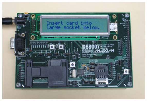
The DS8007 EV kit board comes loaded with this smart-card example transaction software. To verify the presence of this software, apply power to the board and observe the display. If the two-screen banner ending with "Insert card into large socket below." is displayed (Figure 1), then the program is loaded. If this banner is not displayed, the program can be loaded into the board's battery-backed SRAM using the MTK software. Application Note 4036 (see above) describes how to load application files. The file to load is Trans.hex, and is contained in the AN4120_SW.zip file downloadable from the ftp website mentioned above.

Immediately after the file is loaded and the bootstrap loader is disconnected, the processor begins running the application. If still connected to the PC, the MTK screen may display the program's RS-232 serial output. This information is for analysis and debug, however, and should be ignored. The user should follow the instructions displayed on the LCD module. If desired, the source code can be analyzed to determine the meaning of the serial output.
After inserting the smart card, the card's current transaction count and account balance are displayed on the LCD briefly. The display then begins to cycle through the transaction options—Debit, Credit, and Initialization—sequentially and changing approximately every two seconds. When the desired transaction is displayed, press the SW4 switch to execute this transaction. The display then shows the action performed. An ending message is displayed, and the user is instructed to remove the smart card. At this point, the transaction cycle repeats waiting for the card to be re-inserted.
Conclusion
The system described in this application note implements a smart-card payment transaction system based on the DS8007 multiprotocol, dual smart-card interface chip and the DS5002 secure microcontroller. An ACOS3 smart card containing 16kB of EEPROM memory is used, and its Read Record and Write Record commands are used to store information in this nonvolatile memory. Feedback is provided to the user through the on-board 2-line by 20-character LCD. Credit and debit transactions are implemented along with a smart-card initialization function. The source code files are available for download, and can form the basis of a real-world system implementation.
Related to this Article
Products
Multiprotocol Dual Smart Card Interface
High-Speed Secure Microcontroller
Secure Microprocessor Chip
Product Categories
Latest Media 21


