Abstract
The DS5250 high-speed secure microcontroller in the 80-pin quad flat pack (QFP) package is a pin-compatible, high-performance upgrade for the DS5002FP. Upgrading from the DS5002FP to the DS5250 provides higher performance, tighter security and an expanded feature set without requiring changes to the existing hardware design.
Benefits of upgrading include faster execution (up to 25MHz on the DS5250), improved triple DES encryption of program memory, and a 4096-bit modular accelerator engine to support public-key cryptography algorithms such as RSA. Expanded internal SRAM, additional clock modes, and dual data pointers increase flexibility when writing application code. Software developed for the DS5002FP can be ported directly to the DS5250 with only minimal changes required.
The DS5250 high-speed secure microcontroller in the 80-pin quad flat pack (QFP) package is a pin-compatible, high-performance upgrade for the DS5002FP. Because the DS5250 supports the same feature set as the DS5002, it can be used as a drop-in replacement for the DS5002FP in existing designs. Software written for the DS5002FP ports to the DS5250 with few or no changes required, easily improving system performance and security while enabling the features available in the DS5250 (Table 1).
Performance
The DS5250 has higher maximum clock frequencies and requires fewer clocks-per-machine cycle than the DS5002FP. Its streamlined core executes single-byte instructions in only four clock cycles instead of the DS5002FP's 12 clock cycles.
A 1kB instruction cache reduces the effect of program memory encryption on execution speed so that, even with 3DES encryption active, the DS5250 shows an average 2.5x performance improvement over a DS5002FP operating at the same clock frequency.
| DS5002FP | DS5250 | FEATURES |
| PERFORMANCE | ||
| 16MHz | 25MHz | Maximum clock frequency |
| 12 | 4 | Clocks-per-machine cycle |
| 25.2 | 8.4* | Average clocks per instruction |
| 0.63 | 3.9* | Average MIPS |
| SECURITY | ||
| 80-bit proprietary algorithm (single byte) | Single DES or 3DES (8-byte block) | Encryption of data in program memory (decrypted in parallel with program execution) |
| No | Yes | Separate encryption for program and MOVX memory |
| None | 4096-bit MAA engine (1024-bit public key modular exponentiation in under 650ms) | Public key cryptography support |
| SDI pin | SDI pin: no battery/battery attach; low temperature (< 60°C)** | Destructive reset (DRS) triggers |
| No | Yes (optional) | Timed access on port write |
| 48 bytes | 1024 bytes | Vector RAM |
| No | Yes | Unique laser ID |
| No | Yes | Secure loader |
| FLEXIBILITY | ||
| 1x, idle, stop | 1x, idle, stop; 2x/4x (crystal multiplier); divide by 1024 (PMM); internal ring oscillator | Oscillator clock modes |
| 1 | 2 | Serial ports |
| 2 | 3 | Timers |
| 2 | 6 | External interrupts |
| No | Hardware and loader ROM | Flash memory support |
| No | Yes** | Real-time clock |
| *Zero stretch cycles, 16-bit standard addressing mode. **100-pin QFP only. |
||
Security
DS5250 external program memory is automatically secured using either single DES or 3DES encryption; data memory can optionally be encrypted. As with the DS5002FP, encryption keys are generated and loaded automatically from the on-board random-number generator. The DS5250 improves security by using separate keys for program and data memory encryption, and by using an 8-byte block encryption for program memory instead of encrypting it byte by byte.
The DS5250 provides 4kB of internal SRAM that can be used as program memory, data memory, or both; 1kB of SRAM can optionally be used as an extended stack.
In addition to DES and 3DES, the DS5250 includes a 4096-bit MAA engine to support public key encryption algorithms such as RSA. The expanded on-chip vector RAM (1024 bytes vs. 48 bytes for the DS5002FP) provides more space to store critical data and code, such as interrupt and reset handlers.
To protect the internal and external memory, the DS5250 triggers a destructive reset (DRS) based on several conditions. As on the DS5002FP, a signal on the SDI pin clears the memory encryption keys, vector RAM, and any external battery-backed memory. Additionally, the DS5250 triggers a DRS in response to a missing or newly attached battery.
The DS5250 programmable evasion features protect against trial-and-error attacks that involve an abnormal (user-selected) number of resets within a short time. When enabled, this security mode responds to a repeated reset attack with increasing delays according to a user-selected time. Depending on the number of resets encountered, the delay time before execution resumes can increase from seconds to hours to weeks. At the highest security level, the DS5250 can respond to a brute-force attack by locking execution permanently inside the ROM, rendering the part unusable until it is completely erased.
Another countermeasure against attacks is optional timed-access restriction on all output port writes. This increases the instruction bytes an attacker would have to encrypt correctly to write a recognizable pattern to an I/O port.
Flexibility
The DS5250 provides an expanded set of on-chip resources over the DS5002FP, which increases flexibility for application and system design. In addition to the increased 1kB of vector RAM, the DS5250 provides 4kB of internal SRAM that can be used as program memory, data memory, or both. Of this internal SRAM, 1kB can optionally be used as an extended stack.
For clock control and power management, the DS5250 provides many features beyond the standard stop and idle modes supported by the DS5002FP. The clock multiplier allows the external crystal frequency to be doubled or quadrupled internally, expanding the range of crystals used to generate a given clock rate and allowing external EMI to be reduced. Power-management mode (PMM) divides the external crystal frequency by 1024 for reduced power consumption during periods when full-speed operation is not required. If rapid response to a serial input or interrupt is required during PMM, the switchback feature can be used to automatically revert to full-speed operation in response to these inputs. Instead of an external crystal input, an internal ring oscillator, which operates at approximately 12MHz, allows rapid exit from stop mode without waiting for the crystal oscillator to warm up.
Requirements for Upgrading a Design to the DS5250
The DS5250 supports most of the DS5002FP features. Exceptions are:
- The DS5250 accesses all external memory (or memory-mapped I/O) using the dedicated data bus (BA14–BA0 and BD7–BD0). Accessing memory using a multiplexed address/data bus on ports 0 and 2 is not supported.
- The program memory cache allows for the fastest possible program execution. The fills and stalls naturally associated with cache operation may therefore affect I/O timing or bit-bang operations.
- Security enhancements to the DS5250 program memory space may complicate bank switching and/or memory overlay schemes. Specifically, features such as the Program Encryption Key Modifier Register and the use of different encryption schemes for program and data memory may require a reassessment of DS5002FP methods of memory map manipulation.
- The DS5250 does not support reprogrammable peripheral controller (RPC) mode.
If the design relies on one of these features, it is possible that some minor modifications must be made to use the DS5250.
Additionally, the timing requirements for the external RAM(s) accessed through the dedicated data bus changed slightly from the DS5002FP to the DS5250. An AC timing analysis will verify that the RAM and the DS5250 are compatible, particularly if the DS5250 runs beyond the DS5002FP's maximum 16MHz.
Porting Software from the DS5002FP to the DS5250
The DS5002FP and the DS5250 share the same instruction set, and most of the special function registers (SFRs) in the DS5002FP have the same location and function in the DS5250. However, a few changes may be required when porting existing DS5002FP software to the DS5250.
Memory Configuration
The DS5002FP and the DS5250 (80-pin QFP only) support two types of external memory configurations when accessing memory through the dedicated address bus.
The multiple-chip configuration in Figure 1 shows the MSEL pin connected to VCC and four 32kB x 8 SRAM devices connected to the dedicated bus. Two devices (enabled by active-low CE2 and active-low CE1) are mapped as 64kB of program memory, and the other two (enabled by active-low CE4 and active-low CE3) are mapped as 64kB of data memory. To select this configuration, use the following SFR settings:
- ACON.1 (AM1) and ACON.0 (AM0) should be set to 0 to select 16-bit addressing mode (for compatibility with existing software).
- MSIZE should be set to 00h to select the 32kB chip size. Note that this register can only be set in ROM-loader mode or user-loader mode.
- MCON.1 (PM) should be set to 1 to select nonpartitioned mode.
- Program memory is automatically encrypted; the PBCC.0 (TDESE) bit selects whether single DES (
TDESE = 0) or 3DES (TDESE = 1) encryption is used for program memory. This bit can only be set in ROM-loader mode or user-loader mode. - DMOS.1 (C3EE) and DMOS.2 (C4EE) should be set to 1 if data memory encryption is desired. Each of these bits controls encryption on one memory device.

Figure 1. In the multiplechip memory configuration external program and data memory are split across four 32kB x 8 SRAM devices.
In the single-chip configuration (Figure 2, the MSEL pin is connected to ground and a single 128kB x 8 SRAM device is connected to the dedicated bus. This device (enabled by active-low CE1) is used for program and data memory, and active-low CE2 and active-low CE3 are converted into two additional address lines. To select this configuration, the following SFR settings should be used:
- ACON.1 (AM1) and ACON.0 (AM0) should be set to 0 to select 16-bit addressing mode (for compatibility with existing software).
- MSIZE should be set to XX001001b to select the 128kB chip size. Note that this register can only be set in ROM-loader mode or user-loader mode.
- Program memory is automatically encrypted; the PBCC.0 (TDESE) bit selects whether single DES (
TDESE = 0) or 3DES (TDESE = 1) encryption is used for program memory. This bit can only be set in ROM-loader mode or user-loader mode. - Data memory is automatically encrypted.
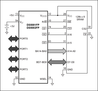
Figure 2. In the single-chip memory configuration, one 128kB x 8 SRAM device holds external program and data memory.
Handling Interrupts
Five of the six interrupt sources supported by the DS5002FP are supported identically on the DS5250. The power-fail interrupt is also supported on the DS5250, but with the following differences:
- The power-fail interrupt vector is located at 33h instead of 2Bh; its priority level (0, the highest) remains unchanged.
- The enable bit for this interrupt is located at WDCON.5 (EPFI).
- The flag indicating that a power-fail event has occurred is located at WDCON.4 (PFI).
Determining Reset Sources
On the DS5002FP, the active-low POR bit (PCON.6) is cleared when a power-on reset occurs, and this bit can be checked by software to determine the cause of a reset. On the DS5250, the POR bit (WDCON.6) performs this function; however, this bit is set (not cleared) when a power-on reset occurs. Both bits require timed-access writes to be reset by software.
The DS5250 streamlined core executes single-byte instructions in only four clock cycles instead of the DS5002FP's 12 clock cycles.
Watchdog Control
The watchdog functions the same on all parts. The following changes and additions apply, however, when controlling the watchdog on the DS5250:
- The watchdog-enable bit is located at WDCON.1 (EWT).
- The watchdog-reset bit is located at WDCON.2 (RWT).
- The flag indicating that a watchdog timer reset has occurred is located at WDCON.2 (WTRF). Unlike the WTR bit on the DS5002FP, this bit must explicitly be written to 0 to be cleared.
- A watchdog interrupt (vector 63h) is available on the DS5250. This interrupt, if enabled by the EWDI (EIE.4) bit, triggers before the watchdog reset occurs, allowing the watchdog timeout to be handled by software if desired. The WD1–WD0 (CKCON.7-6) bits on the DS5250 control the time periods for the watchdog interrupt and reset, but the reset time defaults to roughly the same value as on the DS5002FP.
Random Number Generation
The random number register (RNR) functions the same in all three parts. However, on the DS5250, the bit indicating that a new random number is ready is located at RAMST.0 (RNRF). The time required to generate a new random number on the DS5250 is approximately 30ms.
CRC Operations
The DS5250 supports a new CRC-32 calculation function, and the process to calculate a CRC-16 value is different.
- The DS5250 does not have CRC (C1h), CRCLow (C2h), and CRCHigh (C3h) registers.
- To perform a CRC-16 calculation, first select CRC-16 mode by clearing the CRCNT (RAMST.1) bit to 0. Then write the CRC data values to the CRC1 (B1h) register, allowing at least five machine cycles (or three NOPs between writes) to give the CRC registers time to settle. Once the last value is written, the CRC-16 value can be read from CRC2:CRC1.
- It is no longer necessary to write the CRC LSB byte back into the engine twice to clear the CRC registers. On the DS5240, writing any value to CRC2 automatically clears CRC1, CRC2, CRC3, and CRC4 to 0.
| Device | Active123T |
| Timer2 | CKCON.5 (T2M): Clock Mode Select P1.1 (T2EX), P1.0 (T2): External Inputs T2CON: Flags and Mode Control T2MOD: Mode Control TH2, TL2: Timer Count MSB/LSB RCAP2H, RCAP2L: Timer Capture MSB/LSB |
| Data Pointers | DPH1, DPL1: Data Pointer 1 MSB/LSB DPS: Data Pointer Select |
| CRC: 32 | RAMST.1 (CRCNT): CRC 16/32 Select CRC1, CRC2, CRC3, CRC4: I/O Registers |
| DES Engine | UDESC: DES Engine Control UDESD: DES Engine Data Input/Output |
| Modular Accelerator Engine | MAS0, MAS1: Operation Size Select MACT: Accelerator Control Register |
| User Loader Mode | ACON.6 (ULME): User-Loader Mode Enable PEK1, PEK2, DEK, ROMST, PBCD, PBCC: Encryption/Loading Control |
| Laser ID | BP: Bootloader Password Register |
| Crystal Multiplier and Power Management | PMR: Power Management Register |
| Extended 1kB Stack | ESP: Extended Stack Pointer RAMST.5, RAMST.4: RAMST1 Mode Select |
| Output Port Timed: Access Protection | RAR.3 (TAP): Timed: Access Port Enable |
Conclusion
Many new DS5250 features can be used without any hardware changes. Table 2 summarizes these new features and the SFRs that control them.
The DS5250 feature sets increase security, performance, and flexibility over the DS5002FP. With only a few changes required to port software to the DS5250, upgrading a DS5002FP design is easy.
Upgrading Designs to the 100-Pin QFP
The DS5250 in the 100-pin QFP package provides all the features of the 80-pin package except for pin-for-pin compatibility with the DS5002FP and support for the DS5002FP modes of memory interfacing. It also provides the following features:
- Expanded memory-interfacing options, up to 4MB of program and data memory and 4MB of memory-mapped I/O
- On-board RTC (driven by an external 32.768kHz crystal), useful for time stamping and self-imposed expiration dates
- Temperature sensor that can trigger a DRS in response to a low-temperature attack
- Additional SDI input pin that can be wired to an interrupt to allow a software-controlled tamper response
- Hardware support for external flash memory (loader ROM support included on the DS5250)
For More Information
An overview of the DS5250 high-speed secure microcontroller is available online at www.maximintegrated.com. The confidential data sheet and user's guide require a nondisclosure agreement (NDA) prior to distribution. Contact Maxim Customer Service for more information.
Related to this Article
Products
Product Categories
{{modalTitle}}
{{modalDescription}}
{{dropdownTitle}}
- {{defaultSelectedText}} {{#each projectNames}}
- {{name}} {{/each}} {{#if newProjectText}}
-
 {{newProjectText}}
{{/if}}
{{newProjectText}}
{{/if}}
{{newProjectTitle}}
{{projectNameErrorText}}
Latest Media 21


