Abstract
The MAXQ core is a powerful single-cycle, transport-triggered CPU. This article demonstrates that power by showing how the entire instruction set is built around simple MOVE operations.
The MAXQ processor family are powerful 8-, 16-, and 32-bit, single-cycle microcontrollers that perform multiple operations in one clock cycle. This article explores the internal workings of the MAXQ20 core, and showcases its immense power.
Programmer's Model
The MAXQ20 core is a 16-bit CPU, meaning that all accumulators and most working registers (stack, data pointers, counters) are 16 bits in length. The MAXQ20 can address 64kWords of code space (that is, 64kB instructions) and 64kWords (128kB) of data space (Figure 1).
Note that, for a processor based on the MAXQ20 core, much of this memory space will be vacant. Additionally, because the utility ROM and data RAM reside in the upper 32kB of code space, access to user code in this region requires special features in the core that are beyond the scope of this article.
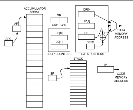
Figure 1. The programmer's model for the MAXQ20 core consists of 16 general-purpose accumulators, two loop counters, and a set of data pointers.
Accumulators
Sixteen registers known as "accumulators" form a general-purpose register array. The register to which the Accumulator Pointer register (AP) points is designated the "active accumulator," which is the target of arithmetic and logical operations. Thus, by changing the value in the AP register, any of the 16 accumulators can be designated the target of an arithmetic logic unit (ALU) operation. The Accumulator Pointer Control register (APC) causes the AP to increment or decrement automatically whenever the active accumulator is accessed, making multiprecision arithmetic simple. In Figure 2, A[0] is the active accumulator, but any accumulator access can make A[1] or A[15] the active accumulator, depending on the value of the APC register.
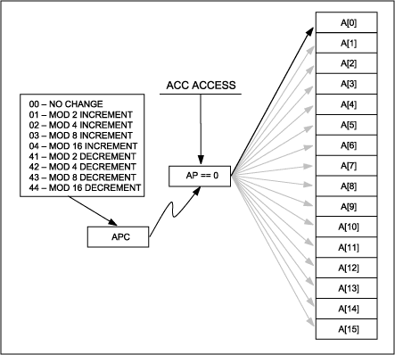
Figure 2. The active accumulator is designated by the AP register, which itself can be modified by accumulator access instructions.
GR Register
The General Register (GR) aids in the extraction of individual bytes from a 16-bit word. A programmer can use GR to assemble bytes into a word: load the low byte into GRL (General Register–Low byte), the high byte into GRH (General Register–High byte), and read the assembled word in GR. Alternately, a programmer can use the GR register to decompose a word into its constituent bytes. A word loaded into GR can be read in a byte-swapped format in GRS (General Register–Swapped). Finally, a byte loaded into the GRL register can be sign-extended to a word by reading GRXL (General Register eXtend Low byte). See Figure 3.
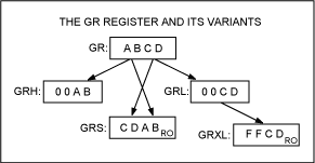
Figure 3. The GR register supports byte extraction, byte-swapping, and 16-bit sign extension.
Loop Counters
There are two loop counters: Loop Counter 0 (LC[0]) and Loop Counter 1 (LC[1]). These registers can be used as general-purpose registers, but are intended as loop counters for decrement and jump if the counters are nonzero (DJNZ) instructions.
Stack
The MAXQ20 core has a dedicated, 16-level internal stack. A stack pointer indicates the next stack location to be used or indicates PUSH or CALL operations.
Data Memory Pointers
The MAXQ microcontroller has three pointers to access data memory. Two, DP[0] and DP[1], are simple 16-bit pointers. The third pointer is formed by adding a base address pointer (BP) to an 8-bit unsigned offset (OFFS).
Note that the data memory, as addressed by one of the three data pointers, is distinctive from the code memory, addressed by the instruction pointer. While all MAXQ processors include a memory management unit (MMU) that allows any memory segment to be treated as code or data, the code and data buses are separate. This separation of buses for code and data fetch operations is a fundamental element of the MAXQ20 technology, and allows simultaneous code and data access in a single clock cycle.
Transfer-Triggered Architecture
By inspecting the programmer's model, one could conclude that there is a conventional instruction fetch-decode unit that loads an instruction, decodes it, and then activates certain elements of the CPU. That, however, would be a misconception. What sets the MAXQ architecture apart from other, more conventional CPUs is the transfer-triggered nature of the MAXQ core.
Transfer-triggering is a technique that allows a simple MOVE instruction to perform every function available in the CPU. While the MAXQ assembler supports more than 30 instruction op codes, one could encode every instruction in the MAXQ instruction set as:
        move Ma[b], Mc[d]
or
        move Ma[b], #immediate_value
where the designation Ma[b] describes register module a and register subdecode b. Simply stated: every instruction—ADD, bit manipulation, reference to external memory—is coded as a move between two registers or as a move of an immediate value into a register.
When a MAXQ instruction is executed, the destination register is loaded with the contents of the source register or with an immediate value. In addition, this transfer of data can trigger other events like incrementing or decrementing a pointer, setting some status bit, or some other function. Hence, the architecture is transfer-triggered. To support this architecture, a large register complement is needed. In the MAXQ20 core, there is a total of 512 register addresses divided into two broad sections: peripheral register space and system register space (Figure 4).
The first six register modules (modules 0 to 5) are dedicated to peripheral registers; the last nine modules (modules 7 to F) are assigned as system registers. (Module 6 is reserved.) While the peripheral register modules change from one type of MAXQ processor to another, the system registers remain the same across all MAXQ processors (Figure 5).
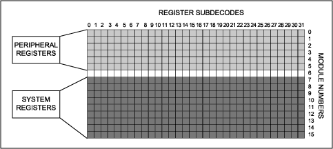
Figure 4. Register assignments in the MAXQ20 core are split into two regions: register banks 0 to 5 are peripheral registers and can change from one MAXQ part to another; banks 7 to 15 are system registers and remain relatively fixed on all MAXQ parts.
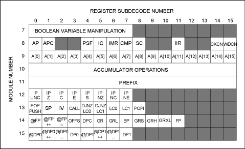
Figure 5. The MAXQ system register map consists of the registers present in all MAXQ20-based processors and additional decodes to implement the instruction set.
Decoding a MAXQ Instruction
Because every MAXQ instruction is really a MOVE, every instruction can be broken down into three fields: a SOURCE field that designates where the data is moved FROM; a DESTINATION field that designates where the data is moved TO; and a format bit that indicates whether the source is an immediate value (FORMAT == 0) or a register designator (FORMAT == 1) (Figure 6).
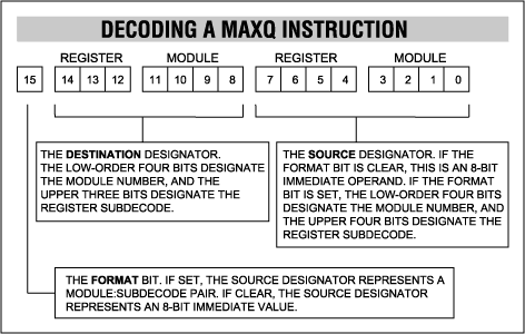
Figure 6. A MAXQ instruction consists of three parts: a source designator, a destination designator, and a source format bit to determine if the source is an immediate operand or a register operand.
Take the instruction op code 0x0923, for example. In this instruction, the FORMAT bit is clear, indicating that the source designator (23) should be treated as an 8-bit immediate value. The destination module is module 9, the accumulator array. Register 0 within that array is the accumulator A[0]. So, the effect of the instruction is to load the value 0x0023 into register A[0]. In this case, there are no side effects associated with either the source or destination designators.
For a second example, consider 0xBF09. In this instruction, the FORMAT bit is set, meaning that the source designator should be interpreted as a register. Module 9 register 0 was covered above: it is the accumulator
Note that in some cases individual locations inside a register module may or may not refer to actual registers. Alternatively, they can refer to an actual register but then cause some side effect to occur when that register subdecode is accessed. For example, let us modify the previous example slightly with 0xAF09. Only the destination subdecode has changed. Now instead of loading the register DP[0], the instruction decrements DP[0] and then begins a store operation to the new memory location to which DP[0] points. That is, the instruction performs an indirect store on a predecremented pointer. In the MAXQ assembler this would be coded as move
The Prefix Register
There are 32 registers per module, but only four bits to select a source register and only three bits to designate a destination register. At first glance, this implies that half the register subdecodes could not be read, and fully three-quarters of register subdecodes could not be written. Fortunately, the MAXQ architecture design works around this. Every MAXQ processor provides a prefix register to supply these additional register address bits, and to provide the upper byte of a word-wide move. See the Module 11—Prefix section for details.
Creating the MAXQ Instruction Set One Module at a Time
The following sections detail the system register modules and how they interact to create all the documented and undocumented instructions. We first investigate the heart of the MAXQ20 core: the accumulator array.
Module 9—Accumulators
The MAXQ architecture supports up to 32 accumulators, although in most variants only 16 are implemented. The accumulators are directly accessed through module 9. Each subdecode within this module represents a single accumulator. Module 9 is conceptually the simplest of the modules, but there are two more modules that affect the accumulator array.
Module 8—System Control
This module contains a number of registers that manage aspects of system operation, such as interrupt control and program status flags. Many of these registers are beyond the scope of this article, so refer to the device specifications for more information. Table 1 lists some of these register modules.
| Sub | Function | S/D | Description |
| 0 | Accumulator Pointer Register | S/D | Designates the active accumulator, i.e., the accumulator that serves as the destination of ALU operations. |
| 1 | Accumulator Pointer Control Register | S/D | Tells the AP how to behave. For this discussion, it is a general-purpose 8-bit register. |
| 4 | Program Status Flags Register | S/D | Contains the flags (carry, zero, equal) that a user may wish to monitor in the main program. The register is usually used as a source, but can also serve as a destination. Note that some of the bits are read-only (e.g., the Z flag is the logical NOR of all the bits in the active accumulator). |
| 5 | Interrupt Control Register | S/D | Manages the interrupt subsystem. |
| 6 | Interrupt Mask Register | S/D | Typically contains bits that mask interrupts at the module level. |
| 7 | Comparator Register | DO | Write-only subdecode. Not really a register, since there is no actual memory behind it. When this subdecode is written, the Equal bit is set in the PSF if the source operand matches the contents of the current accumulator; otherwise, the Equal bit is cleared. |
| 8 | System Control Register | S/D | Contains bits that control aspects of system operation (read/write). |
| 11 | Interrupt Identification Register | SO | Contains a collection of bits that identify the source of an interrupt. |
| 14 | Clock Control Register | S/D | Contains bits pertaining to the system clock. In particular, controls the master clock divide ratio, as well as clock source if more than one source is present in the particular microcontroller. |
| 15 | Watchdog Control Register | S/D | Controls the operation of the watchdog timer. Most MAXQ parts contain a watchdog timer that can reset the processor if it becomes stuck in a program loop. |
The AP and APC registers deserve special attention. The AP register determines which of the accumulator registers is the active accumulator; that is, it designates the target for arithmetic, logic, and bitwise operations. It can point to any accumulator in the array.
The APC register contains a set of bits that define how the AP register is modified following any accumulator operation. Thus, the AP register can be incremented or decremented with the count rolling over on a selectable power-of-two modulus, making multiprecision arithmetic simple.
Module 10—Accumulator Functions
Module 10 is where most of the accumulator's actual work is accomplished. It provides access to the traditional ALU functions and bit-level access to the active accumulator. Module 10 is unique; it behaves differently depending on whether it serves as the source, as the destination, or as both source and destination (Table 2).
| Sub | Function | Description |
| 0 | Active Accumulator | The contents of the active accumulator are moved to the destination and the AP is changed according to the APC. |
| 1 | Active Accumulator | The contents of the active accumulator are moved to the destination and the AP is unchanged. |
If the source is module 10 and the destination is any module other than module 10, the accumulator's contents are moved to the destination. If the subdecode was zero, the AP register is modified according to the bits in the APC register. If the subdecode was 1, the AP register is not modified.
Note that current versions of the macro assembler do not support subdecode 1. This is because there is no mnemonic or modifier to designate subdecode 1. So, the instruction move A[1], ACC will always generate the op code 0x990A and never 0x991A (Table 3).
| Sub | Function | Description |
| 0 | MOVE | The source is moved to the accumulator. |
| 1 | AND | The contents of the source are logically ANDed with the accumulator. |
| 2 | OR | The contents of the source are logically ORed with the accumulator. |
| 3 | XOR | The contents of the source are logically exclusive-ORed with the accumulator. |
| 4 | ADD | The contents of the source are arithmetically added to the accumulator. Overflow out of the MSB sets the carry bit. |
| 5 | SUB | The contents of the source are arithmetically subtracted from the accumulator. Underflow sets the carry bit. |
| 6 | ADDC | The contents of the source and the carry bit are added to the accumulator. |
| 7 | SUBB | The contents of the source and the carry bit are subtracted from the accumulator. |
When module 10 is specified as a destination and the source is either an immediate value or any module other than module 10, the source is routed through the ALU; the destination is taken from the ALU's output, not directly from the source. This is how arithmetic and logical instructions are implemented.
Note that there is no restriction on what may serve as a source register. It can be an immediate value, an indirect memory location, or even a value on the stack or a peripheral register (Table 4).
| Dest Sub | SRC Sub | Function | Description |
| 0 | 0 | MOVE | The contents of the accumulator are moved to the accumulator; logically, an NOP. However, the AP register can be changed. |
| 1 | CPL | The accumulator is complemented bitwise. | |
| 2 | SLA | The accumulator is shifted left one bit; low-order bit is set to zero. High-order bit is copied to carry. | |
| 3 | SLA2 | The accumulator is shifted left two bits; low-order two bits are set to zero. Bit 14 is copied to carry. | |
| 4 | RL | Accumulator is rotated left by one bit, with bit 15 copied to bit 0. Bit 15 is also copied to carry. | |
| 5 | RLC | Accumulator is rotated left by one bit, with bit 15 copied to carry and carry copied to bit 0. | |
| 6 | SLA4 | Accumulator is shifted left four bits; low-order four bits are set to zero. Bit 12 is copied to carry. | |
| 7 | XCHN | The nibbles in each byte of the accumulator are reversed; 0x1234 becomes 0x2143. | |
| 8 | XCH | The bytes of the accumulator are reversed; 0x1234 becomes 0x3412. | |
| 9 | NEG | The accumulator is arithmetically negated. | |
| 10 | SR | The accumulator is shifted right one bit. Bit 15 is loaded with zero. Bit 0 is moved to carry. | |
| 11 | SRA4 | Accumulator is shifted right four bits; high-order four bits are set to zero. Bit 3 is copied to carry. | |
| 12 | RR | Accumulator is rotated right by one bit, with bit 0 copied to bit 15. Bit 0 is also copied to carry. | |
| 13 | RRC | Accumulator is rotated right by one bit, with bit 0 copied to carry and carry copied to bit 15. | |
| 14 | SRA2 | The accumulator is shifted right two bits; high-order two bits are set to zero. Bit 1 copied to carry. | |
| 15 | SRA | The accumulator is shifted right one bit; high-order bit is set to zero. Low-order bit copied to carry. | |
| 1 | Bit | AND C | The carry bit is logically ANDed with the designated bit in the accumulator. |
| 2 | Bit | OR C | The carry bit is logically ORed with the designated bit in the accumulator. |
| 3 | Bit | XOR C | The carry bit is logically XORed with the designated bit in the accumulator. |
| 5 | 0 | C ← 0 | The carry bit is set to zero. |
| 1 | C ← 1 | The carry bit is set to one. | |
| 2 | C ← C | The carry bit is complemented. | |
| 3 | NOP | Guaranteed NOP | |
| 6 | Bit | C ← ACC | The designated bit in the accumulator is loaded into carry. |
| 7 | Bit | ACC ← C | Carry is loaded into the designated bit in the accumulator. |
When both the source and destination designate is module 10, it is either an accumulator-only instruction or a bit manipulation involving the carry bit. In all cases, both the source and destination subdecodes are used to designate the operation.
Destination subdecode 0 is the home of the accumulator-only instructions, including complement, negate, and all shift, rotate, and exchange instructions. Destination subdecodes 1, 2, 3, 6, and 7 involve bitwise loads and operations that use the carry bit. Finally, destination subdecode 5 has the carry-only operations: load 0 and 1 and complement.
Note that one source subdecode of destination subdecode 5 is the designated NOP instruction. While any operation that both has no side effects and addresses a vacant register location will serve as an NOP, a MOVE M10[5], M10[3] is specifically guaranteed to perform no operation in current or future MAXQ devices. This is the op code that is generated (0xDA3A) in all current assemblers for the NOP mnemonic.
Module 12—Instruction Pointer
Module 12 is unique because it contains a number of conditional load operations. If module 12 is used as a source module, the IP is simply copied to the destination designator. But if module 12 is the destination, no operation is performed unless the specified condition is met (Table 5).
| Sub | Description |
| 0 | If source, load the destination from IP. If destination, load IP from the source. |
| 1 | If source, load the destination from IP. If destination, load IP from source only if ACC == 0. |
| 2 | If source, load the destination from IP. If destination, load IP from source only if C == 1. |
| 3 | If source, load the destination from IP. If destination, load IP from source only if the most recent CMP instruction set the EQ flag. |
| 4 | If source, load the destination from IP. If destination, load IP from source only if the high-order bit of the accumulator is set. |
| 5 | If source, load the destination from IP. If destination, load IP from source only if ACC == 0. |
| 6 | If source, load the destination from IP. If destination, load IP from source only if C == 0. |
| 7 | If source, load the destination from IP. If destination, load IP from source only if the most recent CMP instruction cleared the EQ flag. |
Module 12 is also unique because when loaded from an 8-bit immediate source, the source value is interpreted as a signed integer and is added to the previous preincremented contents of the instruction pointer. This addition facilitates relative short jumps, thus offering a significant savings in code size. It also means that any short or long jump instruction can be conditional.
Note that this module supports only simple load and store of the Instruction Pointer register (IP). The CALL instruction is considered a stack instruction that also loads the IP, rather than as an IP instruction that pushes to the stack. Consequently, the transfer for a CALL instruction is in the stack pointer module (module 13). Also, there is no explicit RET instruction; this is cast as a POP IP.
Module 13—Stack Pointer
Module 13 contains not only the stack-pointer-related registers but also the loop counters and interrupt vector. Note that several of the subdecodes are valid only as a destination, and one (subdecode 8) is valid only as a source (Table 6).
| Sub | Function | S/D | Description |
| 0 | PUSH/POP | S/D | If the destination, increment the stack pointer and store the source operand on the stack. If the source, load the value on the stack to the destination and decrement the stack pointer. |
| 1 | Stack Pointer | S/D | Points to the most recently used location on the internal dedicated stack. |
| 2 | Interrupt Vector | S/D | Points to the location in program memory where the interrupt service routine resides. |
| 3 | CALL | DO | Pushes the current IP to the stack, then loads IP from the source operand. Will cause unpredictable results if used as a source operand. |
| 4 | DJNZ LC[0] | DO | Decrements LC[0] and loads IP with the source IF LC[0] != 0. Will cause unpredictable results if used as a source operand. |
| 5 | DJNZ LC[1] | DO | Decrements LC[1] and loads IP with the source IF LC[1] != 0. Will cause unpredictable results if used as a source operand. |
| 6 | LC[0] | S/D | Data is moved to/from loop counter 0. |
| 7 | LC[1] | S/D | Data is moved to/from loop counter 1. |
| 8 | POPI | SO | The value on the stack is copied to the destination, the stack point is decremented, and the IN SERVICE bit is cleared. Primarily used to implement a RETI operation. |
Subdecodes 3, 4, and 5 serve as proxies for the IP register. Subdecode 3 loads the instruction pointer after the incremented instruction pointer is pushed to the stack, thus implementing a traditional CALL instruction. Subdecodes 4 and 5 load a predecremented version of the designated loop counter back to the loop counter, and also load the instruction pointer with the source operand if the predecremented loop counter was nonzero. The source to load into this destination subdecode can be anything; the instruction DJNZ LC[0], A[1] is perfectly valid. In this case, the instruction would decrement LC[0] and jump to the address in A[1] if the result of the decrement operation is nonzero.
Module 14—GR, BP, and DPC
Module 14 contains the DPC register, GR register, and all registers associated with the base pointer and the offset register (Table 7).
| Sub | Function | S/D | Description |
| 0 | @BP[offs] | S/D | Reads or writes the data memory location pointed to by BP+offs |
| 1 | @BP[offs++] | S/D | If source, reads the data memory location pointed to by BP+offs and then increments offs. If destination, increments offs and then stores the source data at BP+offs. |
| 2 | @BP[offs--] | S/D | If source, reads the data memory location pointed to by BP+offs and then decrements offs. If destination, decrements offs and then stores the source data at BP+offs. |
| 3 | offs | S/D | The 8-bit offset register |
| 4 | DPC | S/D | The data pointer control register defines which data pointer is the current source pointer and the word/byte status of each data pointer. |
| 5 | GR | S/D | The 16-bit general register |
| 6 | GRL | S/D | The low-order byte of the 16-bit general register |
| 7 | BP | S/D | The 16-bit base memory pointer |
| 8 | GRS | SO | The byte-swapped version of the GR |
| 9 | GRH | S/D | The high-order byte of the 16-bit general register |
| 10 | GRXL | SO | The sign-extended low byte of the GR |
| 11 | BP[offs] | SO | The sum of the base pointer and the offset |
The Data Pointer Control register (DPC) describes how the data pointers behave. In particular, it contains a bit for each data pointer that defines whether that pointer is operating in word mode or byte mode. It also contains a field that defines which pointer is the current source pointer. This is necessary because the source is accessed when the source pointer is loaded and there is only one bus for operand data.
The GR register is convenient when byte access is required for 16-bit data. Once GR is loaded with 16-bit data, the low- and high-order bytes can be retrieved through the GRL and GRH registers, respectively. The GRS register contains the byte-swapped version of GR; the GRXL register is the same as the GRL register, except that the high byte is the sign extension of the low-order byte.
The Base Pointer register (BP) is one of three data-memory pointer registers in the MAXQ architecture, and the only one to support an offset register. BP typically points to the base of a data structure, and the 8-bit unsigned offset register points to a data element within the structure. Note that the increment and decrement versions of this register modify only the offset register and never the base register.
Module 15—Data Pointers
Module 15 contains two of the three data pointers in the MAXQ architecture. Depending on the subdecode, access to this module will perform a direct or indirect load or store, and may increment or decrement the data pointer following an indirect access. These register subdecodes can be used as either source or destination registers (Table 8).
| Sub | Function | Description |
| 0 | @DP[0] | Reads or writes the data memory location pointed to by DP[0]. |
| 1 | @DP[0]++ | If source, reads the data memory location pointed to by DP[0] and then increments DP[0]. If destination, increments DP[0] and then stores the source data at DP[0]. |
| 2 | @DP[0]-- | If source, reads the data memory location pointed to by DP[0] and then decrements DP[0]. If destination, decrements DP[0] and then stores the source data at DP[0]. |
| 3 | DP[0] | Data pointer 0 |
| 4 | @DP[1] | Reads or writes the data memory location pointed to by DP[1] |
| 5 | @DP[1]++ | If source, reads the data memory location pointed to by DP[1] and then increments DP[1]. If destination, increments DP[1] and then stores the source data at DP[1]. |
| 6 | @DP[1]-- | If source, reads the data memory location pointed to by DP[1] and then decrements DP[1]. If destination, decrements DP[1]. and then stores the source data at DP[1]. |
| 7 | DP[1] | Data pointer 1 |
Module 7—Boolean Variable Manipulation
The Boolean Variable Manipulation (BVM) module (Module 7) allows bit extraction and bit setting/clearing for many registers in a typical MAXQ processor (Figure 7). Note that not all modules have a connection to the BVM machine. Typically, only the peripheral modules connect to the BVM; system registers do not. Consequently, moving data between the BVM and a system register likely causes unpredictable consequences.
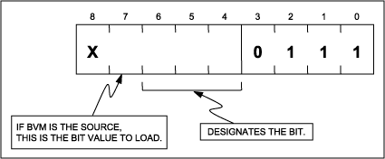
Figure 7. Subdecodes of module 7 designate the bit to extract or replace and, if a source designator, the immediate bit value.
As a destination designator, the BVM serves as a proxy for the carry bit. One bit of the source is extracted and copied to the carry bit. If the BVM is a source designator, the value given in bit 3 of the subdecode (bit 7 of the complete source designator) is copied to the specified bit of the destination.
Note that the BVM only works with bits 0 to 7 of the peripheral register. This is acceptable for most peripheral registers because many registers (I/O ports in particular) are only 8 bits in length. But when accessing 16-bit peripheral registers, only the low-order 8 bits are available.
Module 11—Prefix
The prefix module is a unique feature of the MAXQ architecture that addresses a limitation of all 16-bit microcontrollers. With 16-bit registers, immediate load instructions require a 16-bit operand, meaning that an effective immediate load instruction requires more than 16 bits.
There are several solutions to this limitation, including variable length instructions and registers that allow independent access to the low and high bytes (the MAXQ GR register is an example of this). None of the solutions is ideal because they complicate decode logic or involve new registers (Figure 8).
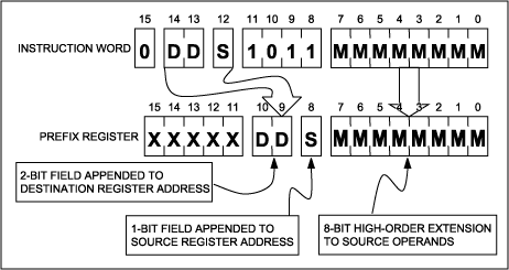
Figure 8. When the prefix register is a destination, the 8-bit immediate source provides the high-order byte for 16-bit immediate operands; the destination subdecode provides additional bits to permit addressing of all 32 registers in each module for both source and destination operands.
The prefix mechanism improves on this process in two ways. First, by prefixing only those instructions that specifically require additional bits, the mechanism saves code space and execution time. And second, by providing additional bits not only for immediate operands but also for register designators, the mechanism preserves the overall architecture while extending the size of the register space.
Remember that while there are 32 registers per register module, only four bits designate a source register and only three bits designate a destination register. The prefix mechanism provides these additional bits.
The prefix mechanism is unique in several ways. Firstly, certain bits in the destination part of the instruction are used as immediate source bits for accessing register subdecodes above 15 for source addresses and above seven for destination addresses. In this way, a single prefix instruction can provide access from any register or immediate value to any register subdecode.
Secondly, the prefix register is unique because any value loaded into it survives for one clock cycle only. After that, the register is automatically cleared to zero. This means that any move to the prefix register must be the instruction immediately before the instruction to be modified by the prefix register. It also means that the prefix instruction is noninterruptible. If an interrupt occurred following a prefix operation, the prefix information would be lost when the interrupt returned to the main function.
As shown in Figure 9, bits from the prefix register go to the source designator, destination designator, and immediate value. So, while most instructions execute in a single cycle, two cycles are required for instructions that: address a destination register subdecode greater than 7; address a source register subdecode greater than 15; or load an immediate value greater than 255.
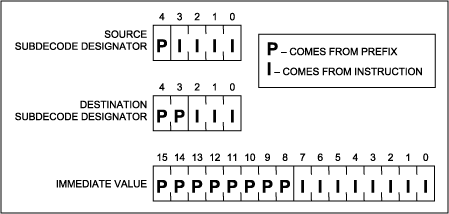
Figure 9. The prefix register provides the additional bits needed for 16-bit immediate operands and to address all 32 registers in each module as both source and destination.
To illustrate this process, consider the instruction move A[0], #010h. As this is moving an immediate value to module 9 register 0, the assembler would create the following op code: 0910. But if the instruction were move
Without the prefix instruction, the op code 2920 would translate to move A[2], #020h. But the prefix adds a bit to the destination specifier and additional bits to the immediate value, allowing the processor to load any value to any register subdecode and never taking more than two cycles.
A Few Examples
The distinctive MAXQ20 core architecture allows some operations that are simply unavailable in other processors.
Vectored Interrupts
The MAXQ20 core has only one interrupt vector register, a factor some may consider a limitation. But consider a system with two external interrupts, in which device A is connected to port 0 bit 0, and device B is connected to port 0 bit 1. Now interrupt selection can be as simple as jump PI0. And at address 0, the code is:
        0000: IRET
        0001: jump SERVICE_DEVICE_A
        0002: jump SERVICE_DEVICE_B
        0003: jump SERVICE_DEVICE_A
In this example, device A has priority in interrupt servicing. That is, if both interrupt request lines are active (port 0 has both bits 0 and 1 active) device A is serviced. At the end of the interrupt service routine, presumably device A will no longer be active and device B can be serviced.
Task Manager
In many applications, it is desirable to cycle through a list of tasks to create a crude type of multitasking environment. This is useful when preemption is not required (or undesirable for real-time reasons). The MAXQ architecture makes this kind of procedure simple:
task_wheel_init:
        move dp[0], #task_list
task_wheel:
        move dp[0], dp[0]
        jump @dp[0]++
.
.
.
task_list:
        dw      task_01
        dw      task_02
        dw      task_03
        dw      task_wheel_init
In this example, DP[0] points to a list of tasks. In the task_wheel routine, DP[0] is selected as the source pointer and then the instruction pointer is loaded from a list of tasks. When each task completes, instead of performing a RET, it simply jumps to the task_wheel routine.
The last entry in the table vectors execution to reinitialize the pointer, and the task wheel begins scanning the table once again.
Traversing a List
Often, it is useful to quickly search a list of irregularly sized objects for a tagged entry. This is difficult in some processor architectures since the memory-access functions are removed from the ALU. In the MAXQ, this is a simple task.
| TAG | LEN | Data | |||||||||||||
| 3F | 09 | 00 | 01 | 02 | 03 | 04 | 05 | 06 | 07 | 08 | |||||
| 17 | 0E | 10 | 11 | 12 | 13 | 14 | 15 | 16 | 17 | 18 | 19 | 1A | 1B | 1C | 1D |
| 35 | 07 | 20 | 21 | 21 | 22 | 23 | 24 | 25 | |||||||
For this example, assume the list contains data objects that consist of a tag, a length, and the data string. A routine to traverse this list might look like this:
item_seek:
        move acc, @dp[0]++     ;Get tag
        jump z, item_not_found ;Tag==0 means end of list
        cmp  a[1]              ;A[1] has target tag
        jump e, item_found     ;If item==target, exit
        move acc, @dp[0]++     ;If no match, get data len
        add  dp[0]             ;Add to pointer
        move dp[0], acc        ;Store pointer back
        jump item_seek         ;...and seek next item.
In eight instructions, this routine traverses a list, seeking a match or a zero entry that terminates the list. On an 8MHz MAXQ20 core, this routine traverses one million entries per second.
Conclusion
Even though the MAXQ core is small and apparently simple, its transfer-triggered architecture gives it a significant edge in speed and flexibility. Because peripherals are addressed directly through the register interface, the speed of data transfer through the embedded peripherals can be impressive. Overall, the MAXQ core in any of its forms is an excellent choice for a wide range of microcontroller applications.
Related to this Article
Products
16-Bit RISC Microcontroller-Based Smart Data-Acquisition Systems
Low-Power LCD Microcontroller
16-Bit Mixed-Signal Microcontroller with LCD Interface
Product Categories
Latest Media 21