Abstract
This application note presents the design of a CDMA Cellular-band power amplifier aimed at the Japan market. A PIN Diode switch is used to improve low power performance. The diode is switched at +16dBm giving a PAE increase and ACPR is better than -50dBc. Data is given for 887, 906 and 925MHz at +27dBm, +16dBm and +13dBm.
Additional Information
For English CDMA applications see The MAX2266 Power Amplifier for the CDMA Cellular Band with the PIN Diode Switch
Introduction
The MAX2269 power amplifier is optimized for IS-98-based CDMA cellular telephones operating in the Japanese cellular-frequency band. With optimized efficiency for medium output power, it achieves good efficiency at medium power, resulting in low-average current consumption in typical urban scenarios and longer talk time.
On the standard evaluation board of the MAX2269, a SPDT switch is used. This board achieves 29% PAE at +27dBm output power and 17% PAE at +17dBm output power. But in this application a PIN diode switch is used instead of the SPDT switch. By changing to a PIN diode switch, better power-added efficiency (PAE) at maximum output power is obtained. Using a PIN diode switch with the MAX2269 also provides PAE at medium and low output power levels.
PIN Diode Switch
The PIN diode chosen for this application is Alpha Industries' SMP1321-079. Figure 1 shows the schematic of the PIN diode switch. When the MAX2269 is in high-power mode, SHDN-bar = High, PWR = High, and the PIN diode switches to OFF. In this condition, POUT goes to high impedance. Then when the MAX2269 is in low-power mode, SHDN-bar = High, PWR = Low, and the PIN diode switches to ON. L1 and L3 are choke coils, and L2 is needed for parallel resonance with the internal capacitance of the PIN diode. The PIN diode forward current is determined by R1.

Figure 1.
Figure 2 shows the output matching portion. If the low-power path isn't connected to the high-power path, the MAX2269's performance is almost the same as the MAX2268's performance. The MAX2268 achieves a PAE of over 35%. Poor isolation for the low-power path produces PAE and ACPR degradation. In the high-power mode, good isolation is needed from the low-power path to obtain good performance.

Figure 2.
Performance
The performance results are shown in Table 1. There are three types of data: maximum output power (+27dBm), switching point (+16dBm), and medium output power (+13dBm). When using the PIN diode switch, the PAE at maximum output power is improved because of the high isolation between the two outputs. At maximum output power, the ACPR is better than -47dBc and the PAE is 33% to 35%. At medium output power, the ACPR is better than -49dBc and the PAE is 18% @ 16dBm and 11% @ 13dBm. Idle current is 36mA.
| Frequency (MHz) | Gain (dB) | ACPR (885kHz) (dBc) | ACPR (1.98MHz) (dBc) | PAE (%) | Idle Current (mA) |
| High-Power Mode @ POUT = +27dBm | |||||
| 887 | 26.88 | -47.70 | -59.67 | 33.37 | |
| 906 | 26.68 | -47.86 | -60.71 | 34.20 | 103 |
| 925 | 25.82 | -47.11 | -60.43 | 35.09 | |
| Low-Power Mode @ POUT = +16dBm | |||||
| 887 | 28.12 | -49.15 | -59.26 | 18.95 | |
| 906 | 27.72 | -50.94 | -60.98 | 18.34 | 36 |
| 925 | 27.06 | -53.09 | -62.23 | 17.49 | |
| Low-Power Mode @ POUT = 13dBm | |||||
| 887 | 28.22 | -60.66 | -64.92 | 11.40 | |
| 906 | 27.76 | -60.88 | -65.15 | 11.17 | 36 |
| 925 | 27.06 | -59.42 | -65.34 | 10.75 | |
With the switching point from high-power mode to low-power mode equal to +16dBm, Figures 3 and 4 show measured performance. In the case of a CDMA system, the PAE at medium output power is very important for longer talk time under normal operating conditions. If the MAX2269 is switched between modes at +16dBm, the PAE increases at medium power while the ACPR is better than -50dBc.

Figure 3 and Figure 4.

Figure 5. Test setup.
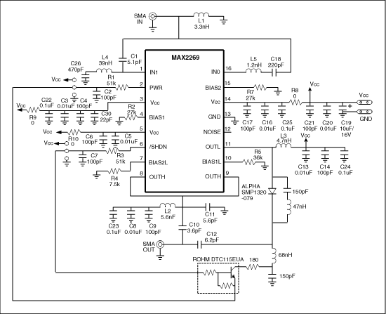
Figure 6. Schematic.
Related to this Article
Products
Product Categories
{{modalTitle}}
{{modalDescription}}
{{dropdownTitle}}
- {{defaultSelectedText}} {{#each projectNames}}
- {{name}} {{/each}} {{#if newProjectText}}
-
 {{newProjectText}}
{{/if}}
{{newProjectText}}
{{/if}}
{{newProjectTitle}}
{{projectNameErrorText}}
Latest Media 21


