Abstract
This application note shows how to implement an uncommitted, isolated SPST (single-pole/single-throw) bipolar power switch that can be used to generate transients of up to 200A and 75V. The switch can be used for testing power supplies and power-supply ICs. Designed for testing fast circuits, the switch achieves turn-on and turn-off times in the tens of nanoseconds.
Introduction
A common problem in testing power circuits in general and power-supply ICs in particular is the need for switches capable of generating the transients and handling the large current and voltage impulses required. Such switches must be capable of connecting to a variety of circuit topologies, depending on the type of power supply under test and its application.
In some cases, it is possible to use a commercial test load; otherwise, it is necessary to develop a one-of-a-kind test setup. If one side of the switch connects to a power-supply common that happens to be the system common as well, the setup design is simple. If not, a custom switch driver needs to be designed, which can be quite complicated. A switch versatile enough to perform most power-supply transient fault tests would be very useful. An outline of the specifications for such a switch should include the maximum voltage and current ratings, as well as the test needs of most of the medium-range power supplies currently on the market.
The switch should have a current capability exceeding 100A and be able to sustain an open-circuit voltage of at least 75V. It must be bipolar both for current carrying and voltage holding, because some tests generate ringing currents and some power circuits produce bipolar outputs. Turn-on and turn-off speeds should be in the tens of nanoseconds to allow observation of the response of fast circuits. Series resistance of the switch must be low. Series inductance must also be very low, which implies a physically small design with a short current path. Last but not least, the switch must be galvanically isolated and have very low output-to-ground capacitance—an essential attribute if the switch is to be inserted in circuits without distorting their performance or response.
Circuit Description
Figure 1 illustrates a switch that satisfies most items in the wish list above. It is implemented with a digital isolator coupler whose side-to-side capacitance is less than 1pF. It has a total propagation delay of 80ns and an output rise time of approximately 40ns. The output stage consists of two low-RDSON MOSFETs capable of handling 75V, 200A transients of either polarity.
The switching element (the two output MOSFETs in antiseries connection) has a 7mΩ series resistance and 25nH series inductance. In the ON state, it behaves as a linear resistor for currents of both polarities (including zero crossover) and, therefore, introduces no harmonic distortion, performing as a metallic contact.

Figure 1. This circuit enables a 5V logic signal to control an uncommitted (isolated) power switch (Q1–Q2) capable of handling 200A pulses at 75V.
For low-resistance loads that draw currents greater than 50A, the switching rise time (defined as the ON transient) is determined mostly by the series inductance. For lower-current ranges, the rise time is below 40ns and the fall time (OFF transient) is primarily a function of the load impedance.
The power supply for the isolated (switch) side of the circuit is a set of three series-connected 3V lithium-coin primary cells (CR2025 manganese-dioxide lithium cells). For switching rates of a few kilohertz, the 170mAh nominally available from this battery type should support continuous use for more than a month. For normal test-bench applications, the battery life should be around three months, if left permanently connected.
The input is a 0V-to-5V digital signal whose only requirements are rise and fall times of less than 20ns and a minimum pulse width (ON or OFF) of 50ns. When conducting less than 18A, the switch can be left in the ON or OFF state indefinitely.
In Figure 1, IC1 and IC2 form an edge detector that applies a narrow positive pulse to either side of the primary of T1 depending on the sign of the input edge. The other side remains low. T1 pulse polarity, then, depends on the polarity of the input-signal edges applied to the circuit. The secondary of T1 connects across a noninverting logical buffer (input to output) formed by one half of a dual, low-side, power-MOSFET driver (IC3). This buffer behaves as a bistable circuit (a flip-flop) that is set in response to a positive pulse at the primary of T1 and reset in response to a negative pulse. The bistable circuit output is then a replica of the circuit input (the digital input signal applied to the edge detector).
The other half of IC3 and the two drivers from IC4 are all connected in parallel. Their inputs connect to the bistable output, and their outputs, connected in parallel, drive the gates of two low-RDSON power MOSFETs (IRFB3077). The two MOSFETs are connected in antiseries with drains to the outside switch power connections, the two gates connected together, and the two sources connected together. The parallel connection of the three drivers enhances the switching speed of the power MOSFETs, because each one of the IC2–IC3 halves can deliver 4A of peak gate current, which is 12A for the three combined. The MOSFET sources connect to the negative side of the battery.
The input logic of the MAX5048 allows easy implementation of the edge detector, and the lower static power consumption of the MAX5054s (used as power-transistor drivers) extend the battery life. Consequently, similar but different IC drivers are included on the low side (control and isolation, IC1 and IC2) and the high side (power drivers, IC3 and IC4).
Figure 2 shows an equivalent circuit for the power switch, including the main parasitic components. As for all power circuits, the switch's continuous power-handling capability depends on the heatsinking provided. Because the inclusion of a heatsink would add considerably to the parasitic output capacitance, however, this design does not include a heatsink. As compensation when handling 200A pulses, the pulse widths must be limited to 8ms and the switching duty cycle limited to a maximum of 0.5%. For 80A transients, the pulses are not package limited and, therefore, can last longer (up to 50ms), but the duty cycle for 80A transients should not exceed 3%.
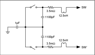
Figure 2. This is a power-switch circuit that is equivalent to the Figure 1 circuit but includes the main parasitic components.
When switching an unclamped inductance at room temperature, the Figure 1 circuit's energy-absorption capability is 280mJ in a single nonrepetitive pulse, or 200mJ/pulse with a maximum 1% duty cycle.
The coupling transformer is designed for minimum size and interwinding capacitance: one turn in the primary and two in the secondary, wound around a Fair-Rite 2643000801 7.5mm × 7.5mm ferrite bead. The transformer construction also sets the maximum-allowable voltage difference between the switched load and the switch-control circuitry. It can easily withstand 1kV when constructed with normal magnet-wire insulation, and more than 1kV if the wire is insulated with teflon or a similar high-quality, high-dielectric rigidity insulation. For higher voltage isolation, all other aspects of the packaging design should also be reviewed.
T1's ferrite core must be considered conductive; therefore, it must not be allowed to contact both sides of the switch at the same time. The switch has no interlock protections, so before using it the condition of the lithium battery must be verified. Circuitry has not been included to guarantee the state of the switch (ON or OFF) when power is applied. Therefore, the power supply for the switch must be turned on before turning on any other power source for the setup. Because the switch state is forced by the first transition applied at the input, the switch should be cycled ON and OFF at least once before applying power to the rest of the setup.
Test Results
In Figures 3–5, the top waveform is the digital input and the bottom waveform is a 5µs pulse observed across a 0.25Ω resistive load, connected by the switch to a 50V power supply. Because the waveforms are voltages developed across a short, very low-inductance film resistor, they closely represent the switch-current waveforms. The approximate 200A pulse shape of Figure 3 is influenced both in its overshoot and its rise time (60ns to 80ns) by parasitic inductance and capacitance in the high-current path. Figure 4 shows the rise time and ON propagation delay of that pulse; Figure 5 shows the fall time and OFF propagation delay. Figures 6–8 show the same waveforms for a 5Ω load and 10A pulse, operating with the same 50V supply. The resulting rise time is closer to the MOSFETs' intrinsic switching rise time of 30ns to 40ns, as limited by the package and the source inductance.

Figure 3. From Figure 1, a 5µs pulse (2), in response to the control signal (1) appears across a load consisting of a 0.25Ω resistor in series with a 50V power supply.

Figure 4. Rise time and ON propagation delay from Figure 3, viewed at a 40ns/cm sweep rate.

Figure 5. Fall time and OFF propagation delay from Figure 3, viewed at a 40ns/cm sweep rate.

Figure 6. From Figure 1, a 5µs pulse (2), in response to the control signal (1), appears across a load consisting of a 5Ω resistor in series with a 50V power supply.

Figure 7. Rise time and ON propagation delay from Figure 6, viewed at a 40ns/cm sweep rate.

Figure 8. Fall time and OFF propagation delay from Figure 6, viewed at a 40ns/cm sweep rate.
Summary
This application note illustrates the design for an SPST bipolar power switch that simplifies power-supply testing. Capable of withstanding the large current and voltage impulses generated during switching transients, this switch can be used to test most of the medium-range power supplies on the market. It can handle 75V, 200A transients of both polarities; it achieves turn-on and turn-off times in the tens of nanoseconds; it features low series resistance and very low series inductance; and it is galvanically isolated with very low output-to-ground capacitance.
A version of this article was initially published in the February 2007 issue of Power Electronics Technology Magazine.
Related to this Article
Products
7.6A, 12ns, SOT23/TDFN MOSFET Driver
4A, 20ns, Dual MOSFET Drivers
Product Categories
Latest Media 21


