S-Parameter Measurements and Stability Analysis for the MAX2640 LNA
Abstract
Stability analysis of the MAX2640 LNA is performed using S-parameter measurements. Multiple test cases confirm the validity of the S-parameter data and that the device is stable up to 5GHz. This note recommends the amount of inductance required on the VCC line for optimum stability. It also summarizes the performance at 315MHz for an automotive keyless-entry application and the match required.
Introduction
For this application note we made S-parameter measurements on the MAX2640 LNA and then conducted a stability analysis using those S-parameter measurements. When we matched the LNA for 315MHz operation, the validity of the S-parameter measurements was confirmed. The resulting analysis will show that the device is unconditionally stable up to 5GHz. We will, finally, recommend the amount of inductance required on the VCC line for optimum stability.
MAX2640 LNA at 315MHz
The performance of this device at 315MHz is summarized in Table 1 below. Figure 1 shows performance vs. frequency.
| Parameter | Customer Target | MAX2640 | ||||
| ICC (mA) | < 2 | 3.5 | ||||
| Gain (dB) | > 13 | 17.4 | ||||
| Noise Figure (dB) | < 2 | 1.4 | ||||
| Input P1dB (dBm) | Not specified | -26 | ||||
| Input IP3 (dBm) | -10 | -17.25 | ||||
| S11 (dB) | Not Specified | -10.5 | ||||
| S22 (dB) | Not Specified | -19.3 | ||||
| (f = 315MHz, VCC = 3V)
Note: Input Power = -30dBm per tone |
||||||

Figure 1. MAX2640 LNA performance vs. frequency for 315MHz application.
S-Parameter Measurements
Test Setup
Two evaluation (EV) kits and a network analyzer (HP8753D) were used to measure the S-parameters for the MAX2640. We removed the IC in the first EV kit (kit #1) and used that kit for calibration. We kept the IC but no matching components in the second kit (kit #2), and used this kit to perform the actual measurements.
- A full 2-port calibration was performed up to the ends of the cables connected to the analyzer.
- When we measured the S-parameters of the IC without matching components in kit #2, a short was placed at the points in kit #1 where the input and output pins of the MAX2640 would be soldered. (See Figure 2 below).
- The port extensions on the network analyzer were adjusted until the impedance at both the input and the output were as close to a short as possible at 315MHz. Using this calibration we measured the S-parameters at the device's pins in kit #2.
- We then modified kit #1 by moving the short to the point where the last matching component would be placed. Once again, the port extensions on the network analyzer were adjusted until the impedance at both the input and the output were as close to a short as possible at 315MHz.
- Next the matching components were returned to kit #2. The IC's S-parameters together with the matching components were measured on the bench.
- To confirm the validity of the S-parameters taken for the IC only (step 3 above), the S-parameters were put into an ADS (microwave simulation software), and models for the matching components and transmission lines were added. We also added a 0.5pF capacitance at the input and output pins to model the parasitics present on the board. (Figure 18 in the Appendix diagrams the ADS simulation.) We then compared the performance curves for this setup with the S-parameter data taken of the IC together with the matching components on the board itself (step 5 above).

Figure 2. Calibration circuit used for measuring the S-parameters of the MAX2640.
Test Results
The labeling for the curves in Figure 3 through Figure 8 is defined as:
- MAX2640_Epcos_1GHz_simulation: the simulation using the S-parameters of the IC only, as measured on the bench, and with the matching components added in ADS.
- MAX2640_Epcos_1GHz_bench: as measured on the bench after adding the matching components to the board itself.

Figure 3. S11 (dB) comparison between simulation and bench measurement.

Figure 4. S11 (phase) comparison between simulation and bench measurement.

Figure 5. S22 (dB) comparison between simulation and bench measurement.

Figure 6. S22 (phase) comparison between simulation and bench measurement.

Figure 7. S21 (dB) comparison between simulation and bench measurement.

Figure 8. S21 (phase) comparison between simulation and bench measurement.
The data above show that both the magnitude and the phase performance for the two test cases are very similar. Except for small shifts in frequency, the simulation (using the S-parameters of the IC only, measured on the bench with the matching components added in ADS) is very close to the actual bench performance (measured on the bench after adding the matching components to the board itself). It can, therefore, be concluded that the S-parameters measured for the MAX2640 are reliable and can be used for simulation and stability analysis.
Note: S12 measurements could not be made for the test where the matching components were added to the board itself. The magnitude of that signal was so low that the analyzer could not make any accurate measurements. Therefore, S12 magnitude and phase curves have not been included in the above plots.
Stability Analysis
To do the stability analysis on the MAX2640, we now measured the S-parameters from 100MHz to 5GHz using the same procedure described above. Three tests cases were performed: first, with 9mm of transmission line present between the VCC pin of the MAX2640 and the decoupling capacitors; second, with the capacitors placed as close to the VCC pins as possible; and third, with the capacitors positioned 5mm away.
First Test Case
We placed the decoupling capacitor 9mm from the MAX2640's VCC pin. The width of the transmission line was 42mil. This was a 4-layer, 50Ω, controlled impedance board; the dielectric material was FR4, 1oz copper with a dielectric constant of ~ 4.5. The dielectric thickness between the top layer and internal ground plane (layer 2) was 24 mil. The inductance seen from the VCC pin was simulated using this information. The resulting data was about j5.5Ω at 315 MHz, which is equivalent to a 2.5nH inductor. Figure 9 shows the stability measurement, stability factor, source stability factor, and load stability factor for the IC only. Figure 10 is the source and load stability circles.

Figure 9. Stability measurement, stability factor, source stability factor, and load stability factor for the first test case.

Figure 10. Source and load stability circles for the first test case.
Second Test Case
For this case we placed the capacitors as close to the VCC pins as possible. Now the length of the transmission line was 40mil and the inductance seen was about j0.6Ω at 315MHz, equivalent to a 0.3nH inductor. Figure 11 below graphs the stability measurement, stability factor, source stability factor, and load stability factor. Figure 12 plots the source and load stability circles.

Figure 11. Stability measurement, stability factor, source stability factor, and load stability factor for the second test case.

Figure 12. Source and load stability circles for the second test case.
Third Test Case
We now placed the decoupling capacitor 5mm from the MAX2640's VCC pin; the width of the transmission line was 42mil, about j3Ω at 315 MHz and equivalent to a 1.5nH inductor. Figure 13 below graphs stability measurement, stability factor, source stability factor, and load stability factor for the IC only.

Figure 13. Stability measurement, stability factor, source stability factor, and load stability factor for third test case.
Figure 13 shows that the stability factors for the three cases are all greater than 1, and that the stability measurement is positive for the entire frequency range. This data meets the requirements for unconditional stability. The stability circles, moreover, are outside the Smith Chart for all frequencies.
The data for the first test case show that the stability factors are safely above 1 in the 2.5GHz to 4.5GHz frequency range, but approaches unity at 5GHz. This indicates that the MAX2640 is conditionally stable above 5GHz. The stability factors for the second test case, however, approach unity in the 2.5GHz to 4.5GHz frequency range, but are safely above unity at 5GHz. This means that the part could be conditionally stable in the 2.5GHz to 4.5GHz range. For the third test case where we placed the capacitors 5mm from the VCC pin, the stability factors are safely above unity in the 2.5GHz to 4.5GHz frequency range and much higher than unity at 5GHz.
From the above analysis, we therefore conclude that for stability, the optimum location for the decoupling capacitors is 4mm to 5mm from the VCC pins.
Schematic and Matching Network
To summarize briefly, a standard network analyzer (HP8753D) was used to measure the S-parameters for the LNA input/output at 315MHz, and an optimum impedance matching circuit was identified using an iterative process of simulation and measurement. This performance at 315MHz and the match required are suitable for an automotive keyless-entry application. The matching was optimized for the best gain and noise figure. The optimum impedance matching circuit is shown below in Figures 14 and 15.
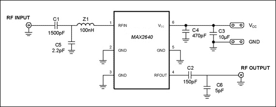
Figure 14. EV kit schematic for the MAX2640 at 315MHz.
| DESIGNATION | QTY | DESCRIPTION |
| Z1 | 1 | 100nH inductor (0603) Coilcraft 0603CS-R10XJBC |
| C1 | 1 | 1500pF ceramic cap (0603) Murata GRM188R71H152KA01B |
| C2 | 1 | 150pF 5% ceramic cap (0603) MurataGRM1885C1H151JA01 |
| C3 | 1 | 10µF ceramic cap (1206) AVX TAJA106D010R |
| C4 | 1 | 470pF 5% ceramic cap (0805) Murata GRM40COG471J50V |
| C5 | 1 | 2.2pF 5% ceramic cap (0805) Murata GRM40COG022D50V |
| C6 | 1 | 5pF 5% ceramic cap (0805) Murata GRM40COG050D50V |

Figure 15. LNA input and output matching network for 315MHz application.
The measurement setup for LNA gain and IIP3 follows. (See Figure 16.)
- A standard two-tone test was used for the IIP3 test.
- Two RF signal generators were connected to the LNA input through a power combiner.
- We setup the first generator (HP8648B) to generate 314.5MHz and the second generator (HP8648B) to generate 315.5MHz (1MHz tone separation). Both tones were generated at -30dBm.
- A spectrum analyzer (Agilent 8562EC) was used to measure the gain and the difference between the wanted tones and the third-order products at the LNA output.
- We used these measurements, along with the input power of each tone, to find the IIP3 for the LNA.

Figure 16. Measurement setup for LNA gain and IIP3.
Measurement Setup for Noise Figure
A noise-figure meter (Agilent N8973A) and a noise source (HP346A) were used to determine the noise figure for the LNA. The setup is diagramed in Figure 17 below.

Figure 17. Measurement setup for noise figure.
Appendix: ADS Simulation Schematic
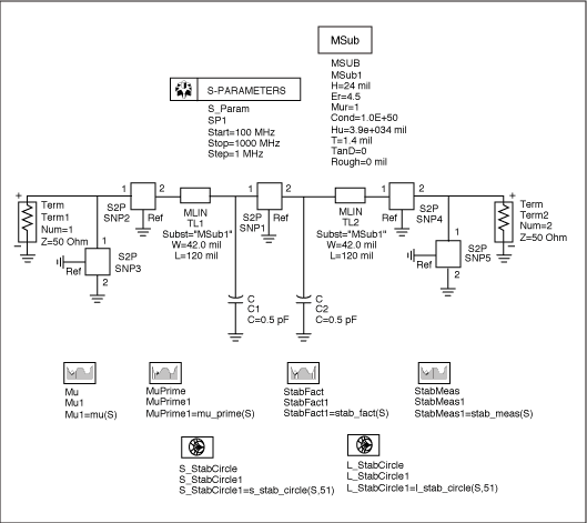
Figure 18. ADS simulation.
Related to this Article
Products
Product Categories
{{modalTitle}}
{{modalDescription}}
{{dropdownTitle}}
- {{defaultSelectedText}} {{#each projectNames}}
- {{name}} {{/each}} {{#if newProjectText}}
-
 {{newProjectText}}
{{/if}}
{{newProjectText}}
{{/if}}
{{newProjectTitle}}
{{projectNameErrorText}}
Latest Media 21


