Selecting External Components for an Automotive Dual Remote Antenna Current-Sense LDO/Switch
Abstract
This application note helps system designers choose the correct external components for use with the MAX16948 dual remote antenna LDO/switch, thus ensuring that automobile-regulated phantom antenna supply and output-current-monitoring circuitry meet performance objectives. An electronic calculator is provided that helps specify the critical external components for the MAX16948, thus reducing design time. The calculator also determines the device's analog output voltage, output current-limit threshold, and output current-sensing accuracies. The calculator includes new automatic Step By Step feature that assists designers with component choice. To use the new automatic feature, click on the Step By Step button relative to the desired section.
Introduction
The MAX16948 is a dual high-voltage low dropout linear regulator (LDO)/switch with output-current sensing. The device provides phantom power over a coax cable to remote radio frequency (RF) low-noise amplifiers (LNAs) in automotive systems with a maximum current of 300mA per channel. The MAX16948 is designed to operate with an input voltage range from 4.5V to 28V (45V load dump tolerant).
The device provides a fixed regulated output voltage of 8.5V or an adjustable 1V to 12V regulated output voltage (LDO mode). The device can also be configured as a switch (SW mode).
The MAX16948 monitors the load current for each channel and provides two analog output currents proportional to the sensed output current (sourced from the SENSE_1; pin). Accurate internal adjustable current limits protect the input supply against both overcurrent and short-circuit conditions.
The device features short-to-battery protection, reverse current detection, input overvoltage and thermal overload shutdown to latch off the internal LDO/switch during these fault conditions. The MAX16948 includes two independent active-low, high-voltage-compatible shutdown inputs (active-low SHDN_) to place each channel in low-power shutdown mode and two active-low open-drain error outputs (active-low ERR_).
External Components for the MAX16948
Figure 1 shows a typical application circuit for the MAX16948. The main external components and their functions are as follows:
- R1_ and R2_ set the regulated output voltage when the device is in LDO mode with adjustable output voltage.
- RLIM_ sets the current-limit threshold.
- RSENSE determines the ADC full-scale input voltage and the output current-sensing accuracy.
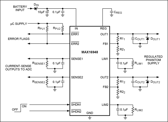
Figure 1. The MAX16948 typical application circuit.
With these external components, the user can easily configure the MAX16948 to work properly for an application. Other external components are necessary. They will be discussed below.
Input Capacitors
Connect a parallel electrolytic capacitor and a low-ESR ceramic capacitor from IN and GND to limit the input-voltage drop during momentary output short-circuit conditions and to protect the device against transients due to inductance on the IN line. For example, use at least a 0.1µF ceramic capacitor in parallel with at least a 10µF electrolytic capacitor if the input inductance (including any stray inductance) is estimated to be 20µH.
When the MAX16948 is operated with input voltage close to the output voltage, as in SW mode operation or LDO mode in dropout, care must be taken to avoid a false reverse-current detection in the presence of a short circuit-to-ground fault. If both channels are enabled and one channel is shorted to ground after startup, the current drawn from CIN may result in a temporary dip in the input voltage, which may trigger the reverse current detection fault. Occurrence of this erroneous fault detection is accentuated at low output current (under 80mA). To avoid this false trigger event, use an input electrolytic capacitor of at least 100µF.
LDO Mode Output Voltage
When used in LDO mode, the device is configurable to provide a fixed 8.5V output or an adjustable 1V to 12V output voltage for each of the two channels. The output voltage can be set to 8.5V by connecting the FB_ pin to REG. In this mode, higher output voltage accuracy is achieved as the tolerance of external resistors does not need to be taken into account.
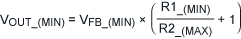
In case a different output voltage is necessary, connect a resistive pider between OUT_, FB_, and GND. Equations to determine the resistive pider value are shown below.

Figure 2. The MAX16948 regulated phantom supply.
The resistors R1_ and R2_ (Figure 2) set the output voltage of the MAX16948. Choose an R2_ standard resistor (R2_(STD)) that is less than or equal to 1kΩ. Calculate the optimum R1_ value with the following equation:

Where VFB_ is the voltage at the feedback pin in regulation (1V nominal).
Once a standard resistor2; R1_(STD)) that is as close as possible to R1_ has been selected, the typical output voltage is:

Considering the tolerance on the resistors (RTOL), the minimum and maximum values of the output voltage are:
And

Where VFB_(MIN) is 0.97V and VFB_(MAX) is 1.03V (over an output current range from 5mA to 150mA). R1_(MIN), R1_(MAX), R2_(MIN), and R2_(MAX) are the minimum and maximum values of R1_ and R2_, respectively:


If the nominal output voltage is too far removed from the desired output voltage, serial or parallel combinations of standard resistors can be used to obtain the optimal resistor pider.
The user can easily determine the value of R1_ by filling in the appropriate section of the MAX16948 Calculator with the desired output voltage (VOUT_), the standard value of R2_, and the tolerance on these resistors. Once the calculator has determined the optimum R1_ value, insert a standard value in the correct cell in order to estimate the VOUT_ range limits. Otherwise, click on the Step By Step button to be guided through the calculator's LDO Mode Output Voltage section.
Connect > 1µF in parallel with 0.1µF low-ESR (< 900mΩ) capacitors between OUT_ and GND for regulator stability. These capacitors should be placed as close to the device as possible. Utilize capacitors with an X7R dielectric to ensure stability over the operating temperature range of the device.
In analogous fashion to the input capacitor, an output capacitor protects the device against transients due to any series inductance in the output. Under no conditions should the voltage on OUT_ go below -0.3V, as indicated in the Absolute Maximum Ratings section of the data sheet. A Schottky diode is required as a clamp if transients are expected to go below ground, especially if an output inductance before the load is present on the PCB. The forward voltage of the selected Schottky diode must be under 0.3V with a forward current equal to the current-limit threshold.3;
Current-Limit Threshold
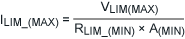
The MAX16948 limits the output current of OUT_ when the voltage on the LIM_ pin reaches the VLIM threshold (2.5V typ). The current sourced from LIM_ is proportional to the load current sourced from OUT_ by a factor called current-sense amplifier (CSA) gain. In this way, the current-limit threshold ILIM_ is set with the RLIM_ resistor.
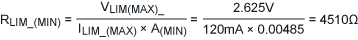
Determine the optimum RLIM_ value using the following equation:

Where ILIM_ is the desired current-limit threshold, VLIM(TYP) is the typical voltage threshold on the LIM_ pin where the output current is limited (2.5V), and A(TYP) is the typical value of the CSA gain (0.005mA/mA).
Select a standard resistor value (RLIM_(STD)) as close as possible to RLIM_. Then the typical current-limit threshold is:

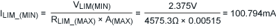
Considering the uncorrelated tolerances, the worst-case current-limit threshold range is between the following two equations:

And
Where VLIM_(MIN) is 2.375V and VLIM_(MAX) is 2.625V; A(MIN) is 0.00485mA/mA and A(MAX) is 0.00515mA/mA (for a typical output current of 100mA); and RLIM_(MIN) and RLIM_(MAX) are the minimum and maximum values of RLIM_ based on the value of RTOL.


If the current-limit threshold range is not suitable, a serial or parallel combination of standard resistors can be used to obtain the optimal range.
The MAX16948 Calculator4 helps the user choose the RLIM_ resistor by selecting the current-limit threshold range limit (ILIM_(TYP), ILIM_(MIN), or ILIM_(MAX)) to calculate the optimum value of RLIM_. This is done by selecting the ILIM_(TYP), ILIM_(MIN), or ILIM_(MAX); the relative current-limit threshold value; and the tolerance on RLIM_. Once the calculator has determined the optimum RLIM_ value, insert a standard resistor value in the appropriate cell in order to estimate the ILIM_ range limits. Otherwise, click on the Step By Step button to be guided through the calculator's Current-Limit Threshold section.
A 0.1µF compensation capacitor (CLIM_) must be placed in parallel with RLIM_ to establish a dominant pole in the current limiting loop. This maintains stability and prevents fast current transients from prematurely triggering the current limit (Figure 3).

Figure 3. The MAX16948 output-current limit.
ADC Input Range and Output Current-Sensing Accuracy
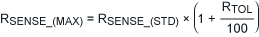
The MAX16948 sources a current proportional to the load current from the OUT_ pin by the CSA gain. This current flowing across RSENSE_ produces a voltage proportional to the output current. With this feature, it is possible to monitor the output current by sampling the voltage on the SENSE_ pin with an ADC.
The ADC full-scale input voltage (VADCFS_) is set with RSENSE_.
Determine the optimum RSENSE_ value using the following equation:

Where ILIM_(TYP) is the typical current-limit threshold calculated in the previous section and A(TYP) is the typical value of the CSA gain (0.005mA/mA).
Select a standard resistor value (RSENSE_(STD)) as close as possible to RSENSE_. Then the typical ADC full-scale input voltage is:

Considering the tolerance on the resistors (RTOL), the minimum and maximum values of the ADC full-scale input voltage are:

And

Where VLIM_(MIN) is 2.375V and VLIM_(MAX) is 2.625V; RLIM_(MIN) and RLIM_(MAX) are been calculated in the previous section; and RSENSE_(MIN) and RSENSE_(MAX) are the minimum and maximum values of RSENSE_ based on the value of RTOL.

Using the Output Current Sensing section of the electronic calculator5, the user can easily determine the RSENSE_ value after inserting the desired ADC full-scale input voltage (VADCFS_) and the tolerance on RSENSE_. Once the calculator has determined the optimum RSENSE_ value, insert a standard value in the corresponding cell in order to estimate the VADCFS_ range limits. Otherwise, click on the Step By Step button to be guided through the calculator's Output Current Sensing section.
However, before using this section, it is necessary to determine the ILIM_ range limits in the calculator's Current-Limit Threshold section.
Place a 0.1µF capacitor (CSENSE) in parallel with RSENSE_ to hold the voltage during ADC sampling cycles (Figure 4).

Figure 4. ADC input range.
Once the voltage on the SENSE_ pin has been measured with the ADC (VADC_), the output current can be estimated by the following formula:

Due to the RSENSE_ tolerance and the parameter spread on the CSA gain, the estimated output current can vary between the following two equations:

And

Replace the value of the CSA gain for a typical output current of 100mA:


Finally, the accuracy of the current measurement made by the ADC is:

This parameter can also be determined in the O.C.S. Accuracy row of the calculator's Output Current Sensing section.
Detection of Open-Load and Overcurrent Conditions
In addition to ADC sampling, open-load or overcurrent conditions can be detected by utilizing external comparators and splitting RSENSE_ into resistive piders (R3_, R4_, and R5_) (Figure 5).

Figure 5. Open-load and overcurrent detection.
The output of the comparators (OC_ and OL_) indicates the operating state of the circuit as shown Table 1.
| OC | OL | STATE |
| 0 | 0 | Normal Operation |
| 0 | 1 | Open-Load Condition |
| 1 | 0 | Overcurrent Condition |
| 1 | 1 | Invalid State |
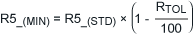
Determine the R5_ value with the following equation:

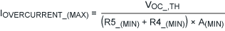
Where IOPEN-LOAD_ is the desired open-load threshold for the current flowing through the LDO/switch, VOL_,TH is the open-load voltage threshold for comparator U2_, and A(TYP) is the typical value of the CSA gain (0.005mA/mA). Once the R5_ resistor value has been calculated, determine the R4_ value using the following equation:

Where IOVERCURRENT_, which must be less than ILIM_(MIN), is the desired overcurrent threshold for the current flowing through the LDO/switch; VOC_,TH is the overcurrent voltage threshold for comparator U1_; and A(TYP) is the typical value of the CSA gain (0.005mA/mA).
Finally, calculate R3_:
R3_ = RSENSE_ - R4_ - R5_
Considering the tolerance of the R3_, R4_, and R5_ standard resistors (RTOL), the minimum, typical, and maximum values of the open-load and overcurrent threshold are:


Where A(MIN) is 0.00485mA/mA and A(MAX) is 0.00515mA/mA (for a typical output current of 100mA); R4_(MIN), R4_(MAX), R5_(MIN), and R5_(MAX) are the minimum and maximum values of R4_ and R5_ based on the tolerance of RTOL.


The user can determine the values of R4_, R5_, and R6_ using the Open-Load & Overcurrent Detection section of the calculator6. Insert IOPEN-LOAD_ (IOL_), IOVERCURRENT_ (IOC_), VOL_,TH, VOC_,TH, and the tolerance on the resistors. Once you have used the calculator to determine the optimum values for R4_, R5_, and R6_, insert standard resistor values in the appropriate cells in order to estimate the IOPEN-LOAD_ and IOVERCURRENT_ range limits. Click on the Step By Step button to be guided through the calculator's Open-Load & Overcurrent Detection section.
Before using the calculator's Open-Load and Overcurrent Detection section, it is necessary to determine the RSENSE_ value in the Output Current Sensing section.
Example Calculations
For these example calculations, we assume an antenna phantom supply application where the supply input voltage is 5V, the typical load current is 100mA, the maximum current-limit threshold value is 120mA, and the output current is monitored with a 3.3V input range ADC.
Assuming that the IN pin of the MAX16948 is directly connected to the battery, the device must be configured in LDO mode to obtain an OUT_ voltage of 5V. For this purpose, the external resistor pider composed of R1_ and R2_ must be dimensioned. Choose a standard value for R2_ (R2_(STD)) less than or equal to 1kΩ and calculate R1_:
R2_(STD) = 750Ω, RTOL = 1% (E96 Series)

Selecting a standard resistor from the E96 Series R1_(STD) = 3010Ω), the output voltage range is:


To obtain a maximum current-limit threshold (ILIM_(MAX)) equal to 120mA, RLIM_ can be calculated after rearranging the ILIM_(MAX) equation:

Selecting a standard resistor from the E96 Series (RLIM_(STD) = 4530Ω), the current-limit threshold range is:


With an ADC input range of 3.3V, calculate the optimum RSENSE_ as follows:

Selecting a standard resistor from the E96 Series (RSENSE_(STD) = 6040O, RTOL = 1%), the ADC full-scale input voltage range is:
VADCFS_(TYP) = RSENSE_(STD) × ILIM_(TYP) × A(TYP) = 6040Ω × 110.375mA × 0.005 = 3.333V
VADCFS_(MIN) = RSENSE_(MIN) × ILIM_(MIN) × A(MIN) = 5979.6Ω × 100.794mA × 0.00485 = 3.104V
VADCFS_(MAX) = RSENSE_(MAX) × ILIM_(MAX) × A(MAX) = 6100.4Ω × 120.685mA × 0.00515 = 3.571V
The accuracy of the output current monitoring is then as follows:

*For more details on these calculations, refer to the MAX16948 data sheet.
Related to this Article
Products
Product Categories
{{modalTitle}}
{{modalDescription}}
{{dropdownTitle}}
- {{defaultSelectedText}} {{#each projectNames}}
- {{name}} {{/each}} {{#if newProjectText}}
-
 {{newProjectText}}
{{/if}}
{{newProjectText}}
{{/if}}
{{newProjectTitle}}
{{projectNameErrorText}}
Latest Media 21


