SD Media Format Expands the MAXQ2000's Space for Nonvolatile Data Storage
Abstract
This article demonstrates how to use the Secure Digital (SD) media format to expand the MAXQ2000's nonvolatile data storage.
The low-power, low-noise MAXQ2000 microcontroller is suitable for a variety of applications. The MAXQ2000 stores nonvolatile data in flash memory and has 32kWords (64kB) flash capacity that is shared with user code space. But what if your application requires more nonvolatile storage? This article demonstrates how to use the Secure Digital (SD™) media format to expand the MAXQ2000's nonvolatile data storage.
Design Considerations for External Storage
The first design considerations for your application are supply voltage and current requirements. In a typical MAXQ2000 application, a dual linear regulator is employed to run the processor core voltage (VDD) at the lowest voltage necessary for the selected design clock rate. The MAXQ2000 VDD supply can be as low as 1.8V. The I/O pins on the MAXQ2000 are supplied by VDDIO, which has an allowable lower range of VDD and an upper limit of 3.6V. Acceptable current draw for external storage is dictated by the current rating of the power supply and, in the case of a battery-powered device, the capacity of the battery system.
Secondly, the number of MAXQ2000 I/O lines used to connect the external storage must be kept to a minimum, while still providing sufficient bandwidth for the intended application. The Atmel AT29LV512 flash chip, for example, requires 15 address lines, eight data lines, and three control lines when interfaced with a host microcontroller. Because the MAXQ2000 does not have an external address/data bus, software would need to control the bus transactions in that example. For some applications, that method is not an efficient use of the MAXQ2000's I/O pins.
SPI™ and I2C-based external flash devices, however, require only three or four interface pins. The MAXQ2000 has a hardware SPI module, while I2C must be implemented on the MAXQ2000 by the user in software (i.e., "bit banging"). This integrated capability means that the SPI-interface is the prime avenue for access to external nonvolatile storage.
SD Memory Card Format
The SD media format is a nonvolatile external memory that satisfies the above considerations for many applications. The SD format is the successor to the "MultiMedia Card" format, or MMC. SD card memories typically operate from 3.3V supplies with modest current requirements. SD card capacities range from a few megabytes up to a maximum capacity of 4GB. This wide range of available sizes provides ample external storage for many applications.
At first glance, SD may not appear to interface easily with the MAXQ2000 due to the former's proprietary shared bus. However, SD inherited MMC's secondary bus format, SPI. Thus, interfacing is simple because the MAXQ2000 contains hardware support for SPI.
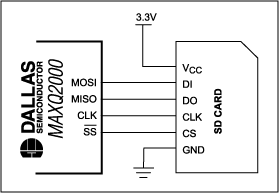
Figure 1. The MAXQ2000 easily interfaces to an SD memory card.
The schematic in Figure 1 shows a typical application circuit. The SD card requires full-duplex, 8-bit SPI operation. Data is clocked into the card's DI pin from the MAXQ2000's MOSI pin, and out of the card's DO line into the MISO pin of the MAXQ2000. Data is clocked simultaneously in and out of the card on the rising edge of the CLK line. Eight extra clocks must be provided at the end of each transaction to permit the SD card to complete any outstanding operations. The input data during these extra clocks must be all ones. Clock rate must be limited to a maximum of 400kHz during the identification phase, but can be increased up to 25MHz once the SD card has been identified.
MAXQ2000 SPI Module
The MAXQ2000 contains a hardware SPI module that is easily configured for the SD card interface. To configure the clock polarity and data length, the SPICF register is programmed to all zeros. This configures the SPI module to latch data on rising clock edges and sets the data length to eight bits. For this application, the MAXQ2000's system clock frequency is 16MHz. In that case, the SPICK register is programmed to 0x28, which results in an SPI clock of approximately 380kHz. The SPI master mode must be enabled by setting the two lower bits of the SPICN register.
SD SPI Data Format
The SD card's SPI protocol is similar to its SD bus protocol. Instead of receiving valid data from the SD card's DO pin at every clock edge, a card with no data to send will hold the DO pin at an idle state of all ones. When the card has data to send back to the host, specialized tokens with a zero start bit are sent before the data. All data transmitted from the SD card is sent immediately after these tokens and is of fixed length. As the receiver has a prior knowledge of the number of bytes to expect, no length bytes are contained in the response. Additionally, as the idle state cannot occur until after the start token and data have been sent, all data bytes are transmitted unaltered and unprefixed. Tokens, as with all other traffic on the bus, are aligned on the 8-bit boundaries of the SPI transaction. Commands and data from the host to the card follow a similar format, with all ones denoting an idle bus. All transactions except status tokens are protected by a cyclic redundancy check (CRC) code appended to the end of data. Two CRC algorithms are provided: CRC-7 for short blocks of data, and CRC-16 for longer blocks of data. The CRC is an optional part of the SD SPI interface, but should be used to guarantee data integrity unless application constraints prevent its use.
Cyclic Redundancy Check
The CRC algorithm is commonly used to detect errors induced by an unreliable communication channel. The selection of a particular CRC is governed by the size of data to be protected. In the case of SD media, CRC-7 and CRC-16 are specified.
The CRC algorithm divides the protected data by a selected divisor and produces a remainder. This division is done without carry logic due to the polynomial math used in the algorithm. As no carries are needed, division can be accomplished with the logical XOR operation. The selected divisor is commonly referred to as the CRC's polynomial. The resulting remainder is then transmitted with the data, and can be used by the receiver to check that the data was not corrupted during transmission.
In the case of CRC-7, the remainder can be calculated using a 7-bit shift register in software. This shift register is initialized to all zeros at the start of the calculation. As each bit (MSB first) of the protected data is shifted into the LSB of the shift register, the MSB of the shift register is shifted out and examined. If the bit just shifted out is one, the contents of the shift register are modified by XORing with the CRC-7 polynomial value 0x09. If the bit shifted out of the shift register is zero, no XOR is performed. Once the last bit of protected data is shifted in and the conditional XOR completed, seven more zeros must be shifted through in a similar manner. This process is referred to as augmentation, and completes the polynomial division. At this point, the CRC-7 value can be read directly from the shift register.
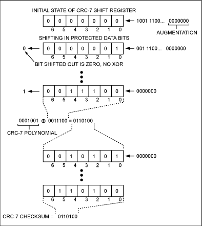
Figure 2. The CRC-7 can be calculated with a shift-register architecture.
When the receiver has all the protected data, the receiver can compute a CRC-7 value over the protected data and compare this with the received CRC-7 value. Should the values differ, the receiver knows that the protected data was corrupted during transmission. If the values match, the receiver knows, with a high degree of certainty, that data integrity was not compromised by the communications channel.
The CRC-16 algorithm can be constructed in the same manner. In this case, the length of the shift register is 16 bits instead of 7, the polynomial value is changed to 0x1021, and the input data is augmented by 16 zero bits.
SD Command Format
Commands are issued to the card in a 6-byte format (Figure 3). The first byte of a command can be constructed by ORing the 6-bit command code with hex 0x40. The next four bytes provide a single 32-bit argument, if required by the command; the final byte contains the CRC-7 checksum over bytes 1 through 5. Table 1 lists important SD commands.
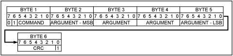
Figure 3. SPI-mode SD commands are issued to the card in a 6-byte format.
| Command | Mnemonic | Argument | Reply | Description |
| 0 (0x00) | GO_IDLE_STATE | none | R1 | Resets the SD card. |
| 9 (0x09) | SEND_CSD | none | R1 | Sends card-specific data. |
| 10 (0x0a) | SEND_CID | none | R1 | Sends card identification. |
| 17 (0x11) | READ_SINGLE_BLOCK | address | R1 | Reads a block at byte address. |
| 24 (0x18) | WRITE_BLOCK | address | R1 | Writes a block at byte address. |
| 55 (0x37) | APP_CMD | none | R1 | Prefix for application command. |
| 59 (0x3b) | CRC_ON_OFF | Only Bit 0 | R1 | Argument sets CRC on (1) or off (0). |
| 41 (0x29) | SEND_OP_COND | none | R1 | Starts card initialization. |
Initializing the SD Card in SPI Mode
At power-up, the SD card defaults to the proprietary SD bus protocol. To switch the card to SPI mode, the host issues command 0 (GO_IDLE_STATE). The SD card detects SPI mode selection by observing that the card select (CS) pin is held low during the GO_IDLE_STATE command. The card responds with response format R1 (Figure 4). The idle state bit is set high to signify that the card has entered idle state. To maintain compatibility with MMC cards, the SPI clock rate must not exceed 400kHz at this stage.
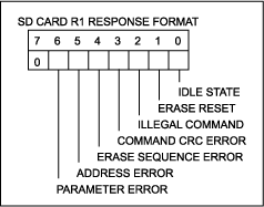
Figure 4. Response format R1 signals the success or failure of the issued command.
Now that the SD card is in SPI mode, the SD specification requires that the host issue an initialization command before any other requests can be processed. To differentiate between MMC and SD cards, SD cards implement an alternative initialization command, to which MMC cards do not respond. Sending command 55 (APP_CMD) followed by application command 41 (SEND_OP_COND) to the card completes this important step. MMC cards do not respond to command 55, which can be used to reject MMC cards as invalid media. This command sequence is repeated until all bits in the R1 response from the card are zero (i.e., the IDLE bit goes low).
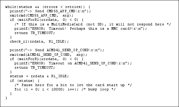
Listing 1. Code must identify SD and MMC cards using SEND_OP_COND.
The SD card contains several important registers that provide information about the SD card. The most important register is the Card Specific Data register (CSD). For our sample application we are interested in the block size and total size of the memory. We must also pay attention to the Card Identification Data register (CID), as it contains details about the cards' manufacturer and serial number. Figure 5 shows the layout of the CSD and CID registers.
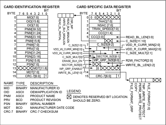
Figure 5. The CSD and CID registers provide information about the SD card.
Examining the SD Card Responses
To read card registers or blocks from the card, we must first understand how the card responds to our inquiries. In SPI mode, the SD card replies to the commands SEND_CSD (9), SEND_CID (10), and READ_SINGLE_BLOCK (17) with a R1 format reply. A start token, the requested data, and finally a CRC-16 checksum over the data follow. We must not assume that the R1 reply and the data start token occur immediately one after the other, as the bus can go to the idle state for some time between these two events. Figure 6 details the data response.
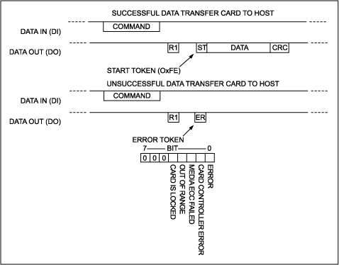
Figure 6. Data transfers from the SD card to the host are prefixed by a start token.
Reading the CSD and CID Register Meta-Data
The SEND_CSD and SEND_CID commands send back register contents used to determine the SD card parameters. These commands return a fixed number of bytes, which corresponds to the size of the CSD or CID register, respectively. The argument contained within the command bytes is ignored by the SD card for these SEND commands.
Reading a Block of Data from the SD Card
Reading a block of data from the SD card is quite simple. The host issues the READ_SINGLE_BLOCK command with a starting byte address as the argument. This address must be aligned with the beginning of a block on the media. The SD card then evaluates this byte address and responds back with an R1 command reply. An out-of-range address is indicated in the command reply.
If the read is completed from the SD media without error, a start data token is sent followed by a fixed number of data bytes and two bytes for the CRC-16 checksum. The start data token is not sent if the SD card encounters a hardware failure or media read error. Rather, an error token is sent and the data transfer is aborted.
Writing a Block of Data to the SD Card
Writing a block of data is similar to reading, as the host must supply a byte address that is aligned with the SD card block boundaries. The write block size must equal READ_BL_LEN, which is typically 512 bytes. A write is initiated by issuing the WRITE_BLOCK (24) command, to which the SD card responds with the R1 command response format. If the command response indicates that the write can proceed, the host transmits the data start token followed by a fixed number of data bytes, and ends with a CRC-16 checksum of the sent data. The SD card returns a data response token indicating the acceptance or rejection of the data to be written.
If the data is accepted, the SD card holds the DO line low continuously while the card is busy. The host is not obligated to keep the card select low during the busy period, and the SD card releases the DO line if CS is deasserted. This process is useful when more than one device is connected to the SPI bus. The host can wait for the SD card to release the busy indication, or check the card by periodically asserting the chip select. If the card is still busy, it will pull the DO line low to indicate this state. Otherwise, the card returns the DO line to the idle state (see Figure 7).
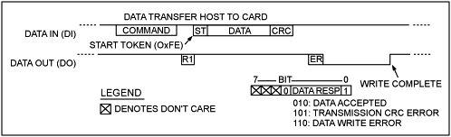
Figure 7. Data transfers from the host to the SD card involve a more complex handshake.
SPI Command and Data Error Detection
The CRC-7 and CRC-16 checksums can be used to detect errors in the communication between the host and SD card. Error detection allows for robust error recovery in the event of physically induced errors such as contact bounce during insertion and removal or nonideal contact-mating situations inherent with detachable media. The use of checksums, by issuing the CRC_ON_OFF (59) command with the lowest bit set in the argument, is highly recommended.
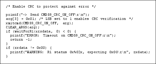
Listing 2. Enabling the CRC checksum is highly recommended.
Conclusion
The SD media card format represents a compact, low-power nonvolatile memory solution for embedded systems. By using the hardware SPI support provided by the MAXQ2000 microcontroller, SD media cards can be accessed with very little overhead. The reference software provided by Maxim demonstrates a minimal implementation, which includes the essential operations required to read blocks from and write blocks to an SD card.
Related to this Article
Products
Product Categories
{{modalTitle}}
{{modalDescription}}
{{dropdownTitle}}
- {{defaultSelectedText}} {{#each projectNames}}
- {{name}} {{/each}} {{#if newProjectText}}
-
 {{newProjectText}}
{{/if}}
{{newProjectText}}
{{/if}}
{{newProjectTitle}}
{{projectNameErrorText}}
Latest Media 20


