Rugged 3.3V RS485/RS422 Transceivers with Integrated Switchable Termination
Rugged 3.3V RS485/RS422 Transceivers with Integrated Switchable Termination
Mar 1 2007
Introduction
Medium and high speed RS485 networks must be terminated to avoid data-corrupting reflections. This means a termination resistor is placed at each end of the bus. Of course, if the network is expanded or reconfigured, the termination resistors must also move. The 3.3V LTC2854 and LTC2855 transceivers eliminate the cumbersome task of shuffling termination resistors. These devices have an integrated termination resistor connected across the receiver inputs that can be enabled or disabled with simple logical control of an input pin, making network configuration and reconfiguration a snap. These devices come in tiny packages and are extremely robust, withstanding ESD strikes of up to ±25kV HBM (LTC2854) on the line I/O pins—the industry’s highest protection level for an RS485 transceiver.
Other features of the LTC2854 and LTC2855 include a receiver with balanced thresholds for excellent duty cycle performance, high input resistance allowing as many as 256 devices to be connected to one bus, and a full failsafe output. The driver offers low power operation, which in conjunction with the receiver and integrated termination resistor, provide a single die impedance-matched network solution. Parts are available in half- and full-duplex configurations in tiny packages including 10- and 12-pin DFN as well as 16-lead SSOP (see Table 1 and photo in Figure 1).

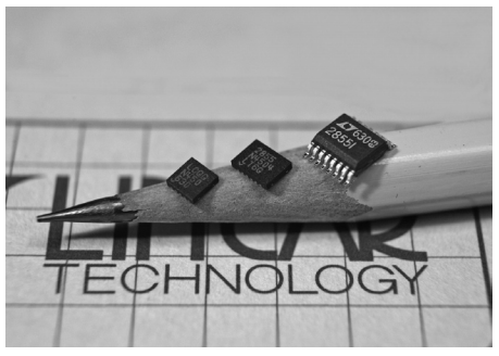
Figure 1. Photograph of the (left to right) LTC2854 3mm × 3mm DFN, LTC2855 4mm × 3mm DFN, and the LTC2855 SSOP
| Part Number | Duplex | Package | Esd On Line I/O (HBM) |
| LTC2854 | Half | DNF-10 | ±25kV |
| LTC2855 | Full | SSOP-16, DFN-12 | ±15kV |
Block diagrams for the LTC2854 and LTC2855 are shown in Figure 2.

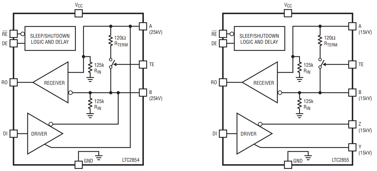
Figure 2. Block diagrams of the LTC2854 and LTC2855
Switchable Termination Differential signals propagating down a twisted pair transmission line are partially reflected when an impedance mismatch is encountered. The reflected signal causes constructive and/or destructive interference on the line that can corrupt data. To prevent this condition and optimize system performance, transmission lines should be terminated at each end with a resistor matching the characteristic impedance of the cable.
The LTC2854 and LTC2855 transceivers integrate this termination resistor so that it can be selectively included or excluded simply by controlling the Termination Enable pin (TE). The resistor is effectively connected across the receiver input pins by setting TE high and disconnected when TE is low or the device is unpowered. This arrangement is nearly ideal from a system management standpoint, especially under conditions where a network configuration changes and the termination resistor needs to be moved to the new end of the bus. In this case, manual removal and placement of a discrete resistor is not necessary; rather the change is controlled digitally with the appropriate selection of TE pins on the LTC2854 or LTC2855.
To illustrate the importance of termination placement, consider the configuration shown in Figure 3 where the effects of network expansion are presented. The initial configuration consists of nodes 1 and 2, made up of LTC2854 transceivers connected with 200 feet of Cat 5 cable. The waveforms in the lower left of the figure show the signal received at node 2, driven from node 1. Both ends of the cable are terminated by setting the TE pins high on both transceivers. The received signal looks clean because the bus is properly terminated.

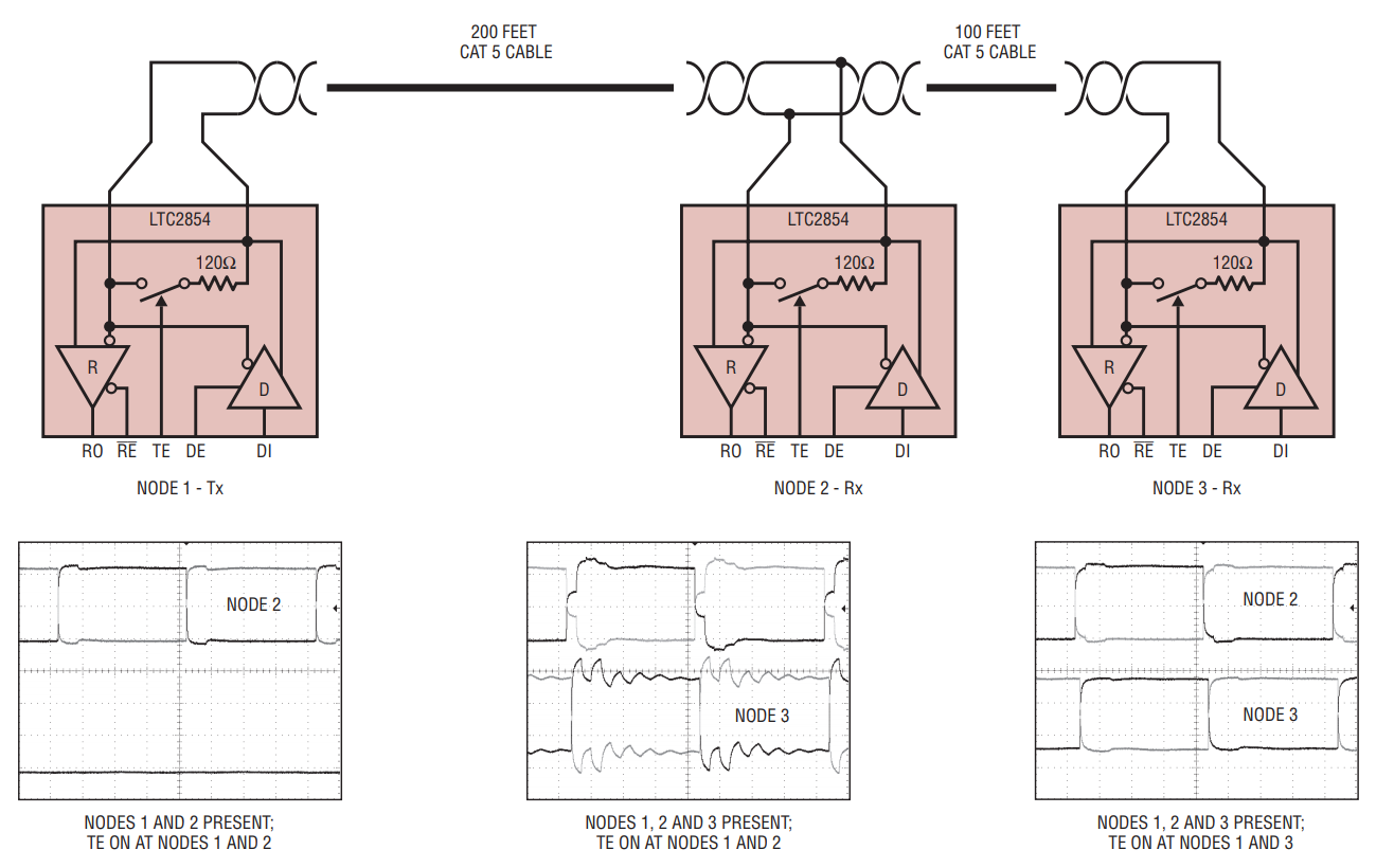
Figure 3. Effects of termination placement with network expansion
A small impedance mismatch between the cable characteristic impedance of 100Ω and the termination resistor of 120Ω, results in a slight bump in the waveform. This effect is minor and the figure serves to illustrate that the termination resistor in the LTC2854 and LTC2855 is compatible with popular low cost 100Ω cables.
The second set of waveforms on the bottom of Figure 3 show the results of introducing a third node to the system through 100 feet of added cable but without moving the termination resistor to the new end location. The waveforms at node 3 and node 2 are both severely distorted from reflections caused by the improper termination. In the third set of waveforms, the termination placement has been corrected by setting TE high at nodes 1 and 3 only, thereby cleaning up the signals received at nodes 2 and 3. The logic-selectable termination resistors in the LTC2854 permit this correction with no physical intervention required.
The termination resistance is well maintained over temperature, common mode voltage and frequency (as illustrated in Figure 4). Furthermore, the termination network adds only insignificant capacitive loading to the receiver pins. The input capacitance on the LTC2855’s A and B pins is approximately 9pF measured to ground and 3.5pF differentially.

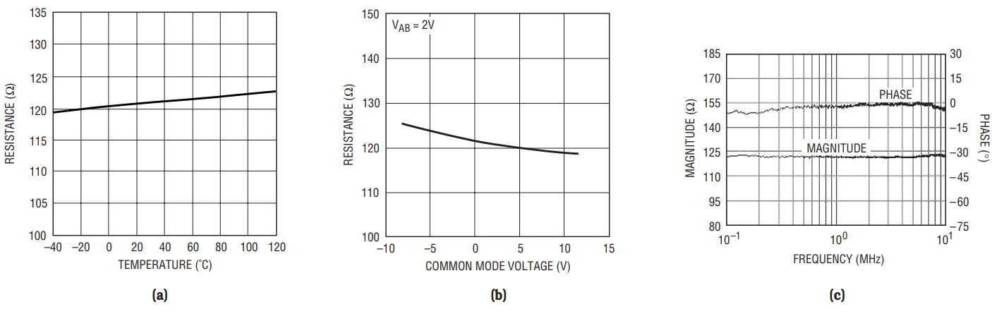
Figure 4. LTC2855 termination resistance vs (a) temperature, (b) common mode voltage, and (c) frequency.
Balanced Threshold Receiver with Full Failsafe
The LTC2854 and LTC2855 feature a low power receiver that draws only 450µA. The single-ended input resistance to ground on each of the receiver inputs is greater than 96kΩ when the termination is disabled. This is eight times higher than the requirements specified in the TIA/EIA-485-A standard and thus this receiver represents a one-eighth unit load. This, in turn, means that 8× the standard number of receivers, or 256 total, can be connected to a line without loading it beyond what is called out in the standard.
The receiver implements a full failsafe design that drives RO high when the inputs to the receiver are shorted, left open, or terminated (externally or internally) but not driven.
A key element of the LTC2854/LTC2855 receiver is that it uses a window comparator with two voltage thresholds balanced around zero for excellent duty cycle performance. As illustrated in Figure 5, for a differential signal approaching from a negative direction, the threshold is +65mV. When approaching from the positive direction, the threshold is –65mV. Each of these thresholds has 20mV of hysteresis (not shown in the figure). This windowing around 0V preserves duty cycle for small inputs with heavily slewed edges. This performance is highlighted in Figure 6, where a signal is driven through 4000 feet of Cat 5e cable at 3Mbps. The top set of traces show the signals coming into the receiver after traveling down the long cable. The middle trace is the difference of the top two signals and the bottom trace is the resulting waveform out of the receiver at the RO pin. It is clear that even though the differential signal peaks at just over ±100mV and is heavily slewed, the output maintains a nearly perfect signal with almost no duty cycle distortion.

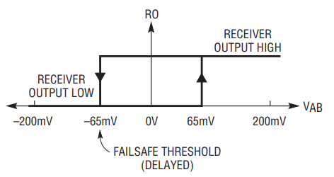
Figure 5. Receiver input threshold characteristics

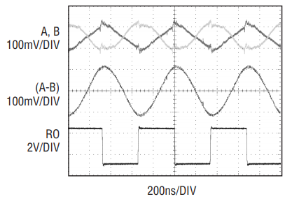
Figure 6. A 3Mbps signal driven down 4000 feet of Cat 5e cable. Top traces: received signals after transmission through cable; middle trace: math showing difference of top signals; bottom trace: receiver output.
Few devices can match this level of performance because the balanced receiver thresholds are at odds with shorted failsafe requirements. Other parts typically include a negative threshold in the receiver so that when the inputs are shorted together (i.e., 0V differential) the receiver output drives high, indicating a failsafe condition. Unfortunately, the negative offset can cause severe duty cycle distortion for small, slow-edge rate signals like those presented in Figure 6.
The LTC2854 and LTC2855 avoid this problem by using a method to detect the shorted failsafe condition that preserves normal signal integrity. In normal operation, the two thresholds shown in Figure 5 are used to determine the receiver output state. However, if the receiver inputs remain between thresholds for more than about 3µs, the receiver output is driven high, reflecting this failsafe condition.
Driver
The differential driver of the LTC2854 and LTC2855 easily delivers RS485/RS422 signals at data rates up to 20Mbps. Figure 7 shows the clean edges and excellent zero crossings of the LTC2854 driver running at 20Mbps into a 54Ω load. Figure 8 shows a single 50ns pulse (equivalent to one bit at 20Mbps) delivered through 100 feet of standard unshielded Cat 5 cable and received by a second LTC2854 transceiver.

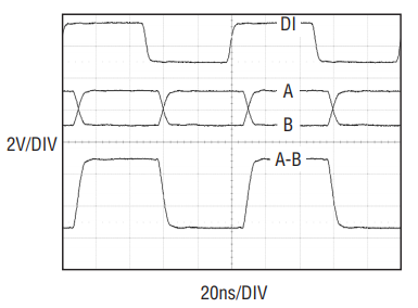
Figure 7. The LTC2854 driver toggling at the maximum data rate of 20Mbps into 54Ω. A and B are the driver outputs.

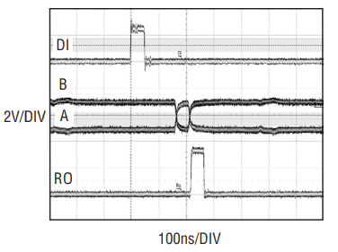
Figure 8. The LTC2854 driver delivering a single 50ns pulse through 100ft of Cat 5 cable, which is received by another LTC2854. Both parts have their on-chip termination enabled. Top trace is the input to the transmitting device and the middle and bottom traces are observed at the receiving part.
Driver outputs have current limiting that offers protection from short circuits to any voltage within the absolute maximum range of (VCC–15V) to +15V, with typical peak current not exceeding 180mA. Additionally, thermal shutdown protection disables the driver, receiver, and terminator if excessive power dissipation causes the device to heat to temperatures above 160°C. When the temperature drops below 140°C, normal operation resumes.
Extreme ESD Protection
The driver output pins and receiver input pins on the LTC2854 are protected to ESD levels of ±25kV HBM with respect to ground or VCC. The full-duplex LTC2855 withstands ±15kV ESD. These protection levels exist for all modes of device operation including power-down, standby, receive, transmit, termination and all combinations of these. Furthermore, the protection level is valid whether VCC is on, shorted to ground, or disconnected.
When a line I/O pin on the LTC2854/LTC2855 is hit with an ESD strike during operation, the part undergoes a short disturbance of duration similar to the ESD event and then fully recovers. The device does not latch up and there is no need to toggle states or cycle the supply to recover. This is true whether the part is in a static state or sending/receiving data and for the full range of ground common mode voltages called out in the RS485 standard. The photo in Figure 9 shows the LTC2854 absorbing the energy from an ESD gun (configured for IEC air discharge) delivering repeated 30kV strikes to the ‘A’ pin while transmitting data. The oscilloscope traces in the background show data toggling happily on the A and B pins before and after a strike, with a positive glitch only during the ESD event. This device can handle many such strikes without damage.

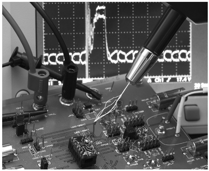
Figure 9. The LTC2854 sending data (see scope traces in background) while hit with multiple 30kV ESD strikes on the ‘A’ pin.
Conclusion
The LTC2854 and LTC2855 break new ground in the world of 3.3V RS485/RS422 transceivers. The inclusion of a selectable termination resistor provides a complete solution to RS485 networking with the ability to remotely configure the network for optimal data transfer. Unparalleled ESD performance provides outstanding ruggedness while a balanced-threshold receiver with full failsafe capability makes this family of small-footprint devices a natural choice for modern RS485/RS422 systems.
About the Authors
Steven Tanghe is an Engineering Design Manager at Analog Devices based in Burlington, Vermont. He has a Ph.D. from the University of Michigan in electrical engineering and MEMs. Steven joined Analog Devices (Linear Techno...
{{modalTitle}}
{{modalDescription}}
{{dropdownTitle}}
- {{defaultSelectedText}} {{#each projectNames}}
- {{name}} {{/each}} {{#if newProjectText}}
-
 {{newProjectText}}
{{/if}}
{{newProjectText}}
{{/if}}
{{newProjectTitle}}
{{projectNameErrorText}}
Latest Media 21


