Read other articles in this series.
Abstract
Bridge circuits are a very useful way to make accurate measurements of resistance and other analog values. This article, the continuation from Part One, covers how to interface bridge circuits implemented with higher signal-output silicon strain gauges to analog-to-digital converters (ADCs). Featured are sigma-delta ADCs, which provide a low-cost way to implement a pressure sensor when utilizing silicon strain gauges.
Introduction
Part one of this topic, application note 3426, "Resistive Bridge Basics: Part One", discusses why resistive bridges are used, basic bridge configurations, and discusses bridges with small-output signals like those made from bonded wire or foil strain gauges. This application note focuses on the high-output silicon strain gauges. This application note, Part Two, focuses on the high-output silicon strain gauges and their excellent fit with high-resolution, sigma-delta analog-to-digital converters (ADCs). Examples of how to calculate the required ADC resolution and the dynamic range for uncompensated sensors are given. This note shows how the characteristics of ADCs and silicon strain gauges can be exploited to create simpler ratiometric circuits and a simplified circuit for applications using current-driven sensors.
Silicon Strain-Gauge Background
The advantage of the silicon strain gauge is its high sensitivity. Strain in silicon causes its bulk resistance to change. This results in signals an order of magnitude larger than those from foil or bonded-wire strain gauges, where resistance changes are only due to the dimensional changes of the resistor. The large signal from silicon strain gauges allows lower cost electronics to be used with them. The cost and difficulty, however, of physically mounting and attaching wires to these small brittle devices has limited their use in bonded strain-gauge applications. Nonetheless, the silicon strain gauge is optimal in MEMS (Micro Electro Mechanical Structures) applications. Using MEMS, mechanical structures can be created in silicon, and multiple strain gauges can be manufactured as an integral part of those mechanical structures. Thus, the MEMS process provides a robust, low-cost solution to the total design problem without the need to handle individual strain gauges.
The most common example of a MEMS device is the silicon pressure sensor, which first became popular in the 1970s. These pressure sensors are fabricated using standard semiconductor processing techniques, plus a special etching step. The special etch selectively removes silicon from the back side of the wafer to create hundreds of thin square diaphragms with strong silicon frames surrounding them. On the front side of the wafer, one strain-sensitive resistor is implanted on each edge of each diaphragm. Metal traces connect the four resistors around an individual diaphragm to create a fully active Wheatstone bridge. A diamond saw is then used to free the individual sensors from the wafer. At this point the sensors are fully functional, but must have pressure ports attached and wires connected before they are useful. These small sensors are inexpensive and relatively robust. There is a negative, however. These sensors suffer from large temperature effects and have a wide tolerance on initial offset and sensitivity.
Pressure Sensor Example
For illustrative purposes, a pressure sensor is used here; the principles involved are applicable to any system using a similar type of bridge as a sensor. One model for the output of a raw pressure sensor is seen in Equation 1. The magnitude and range of the variables in Equation 1 yield a wide range of VOUT values for a given pressure (P). Variations in VOUT exist between different sensors at the same temperature and for a single sensor as the temperature varies. To provide a consistent and meaningful output, each sensor must be calibrated to compensate for part-to-part variations and drift over temperature. For many years calibration was done with analog circuitry. Modern electronics, however, are making digital calibration cost competitive with analog, and the resulting accuracy of digital calibration can be much better. A few analog "tricks" can be used to simplify digital calibration without sacrificing accuracy.
VOUT = VB × (P × S0 × (1 + S1 × (T - T0)) + U0 + U1 × (T - T0))
Where VOUT is the output of the bridge, VB is the bridge excitation voltage, P is the applied pressure, T0 is the reference temperature, S0 is the sensitivity at the T0, S1 is the temperature coefficient of sensitivity (TCS), U0 is the offset or unbalance of the bridge at T0 with no pressure applied, and U1 is the offset temperature coefficient (OTC).
Equation 1 uses first-order polynomials to model the sensor. For many applications it may be necessary to use higher-order polynomials, piecewise linear techniques, or even piecewise second-order approximations with a lookup table for the coefficients. Regardless of which model is used, digital calibration requires the ability to digitize VOUT, VB, and T, as well as a way to determine all the coefficients and perform the necessary calculations. Equation 2 is Equation 1 rearranged to solve for P. Equation 2 more clearly shows the information needed for the digital computation, typically by a microcontroller (µC), to output an accurate pressure value.
P = (VOUT/VB - U0 - U1 × (T-T0))/(S0 × (1 + S1 × (T-T0))
Brute-Force Circuit
The brute-force method shown in the Figure 1 circuit uses a single high-resolution ADC to digitize VOUT (AIN1/AIN2), temperature (AIN3/AIN4), and VB (AIN5/AIN6). These measurements are then sent to a µC where the actual pressure is calculated. The bridge is powered directly from the same power supply as the ADC, the voltage reference, and the µC. A resistance temperature detector (RTD), denoted Rt in the schematic, measures temperature; the input MUX on the ADC allows for measurement of the bridge, the RTD, or the supply voltage. To determine the calibration coefficients, the entire system (or at least the RTD and bridge) is placed in an oven and measurements are made at several temperatures as a calibrated pressure source stresses the bridge. The measurement data is then manipulated by the test system to determine the calibration coefficients. The resulting coefficients are downloaded to the µC and stored in nonvolatile memory.
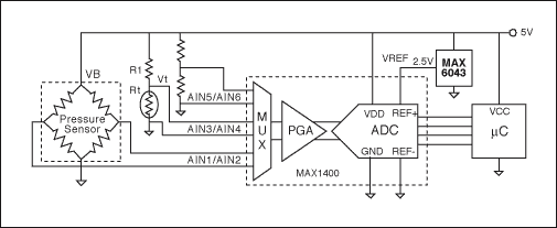
Figure 1. Circuit directly measures the variables needed to calculate the actual pressure (excitation voltage, temperature, and bridge output).
Key considerations in designing such a circuit are the dynamic range and ADC resolution. The minimum requirements will depend on the application and the exact specifications of the sensor and RTD used. For illustrative purposes, the following specifications are used.
System specifications
- Full-scale pressure: 100psi
- Pressure resolution: 0.05psi
- Temperature range: -40°C to +85°C
- Power supply: 4.75 to 5.25V
Pressure sensor specifications
- S0 (sensitivity): 150 to 300µV/V/psi
- S1 (temperature coefficient of sensitivity): -2500ppm/°C, max
- U0 (offset): -3 to +3mV/V
- U1 (offset temperature coefficient): -15 to +15µV/V/°C
- RB (input resistance): 4.5k
- TCR (temperature coefficient of resistance): 1200ppm/°C
- RTD: PT100
- Alpha: 3850ppm/°C (ΔR/°C = 0.385Ω nominal)
- Value at -40°C: 84.27Ω
- Value at 0°C: 100Ω
- Value at 85°C: 132.80Ω
- For more details on the PT100, see Analog Devices application note 3450, "Positive analog feedback compensates PT100 transducer."
Voltage Resolution
The minimum acceptable voltage resolution is based on the smallest response of VOUT to the minimum detectable pressure change. This condition occurs when using the lowest sensitivity sensor at the maximum temperature with the lowest supply voltage. Note that the offset terms in Equation 1 are not factors here because resolution is only dependent on the response to pressure.
Using Equation 1 and the appropriate assumptions from above:
ΔVOUT min = 4.75V (0.05psi/count 150µV/V/psi × (1+ (-2500ppm/°C) × (85°C -25°C)) ≈ 30.3µV/count
Therefore: minimum ADC resolution = 30µV/count
Input Range
Input range is determined by the largest possible input voltage and the smallest, or most negative, input voltage. The conditions that create the largest value of VOUT in Equation 1 are: maximum pressure (100psi), minimum temperature (-40°C), maximum supply voltage (5.25V), an offset of 3mV/V, offset TC of -15µV/V/°C, a TCS of -2500ppm/°C, and the highest sensitivity die (300µV/V/psi). The most negative signal will be with no pressure applied (P = 0), the supply voltage at 5.25V, an offset of -3mV/V, at a temperature of -40°C, with an OTC of +15µV/V/°C.
Again, using Equation 1 and the appropriate assumptions from above:
VOUT max = 5.25V × (100psi · 300µV/V/psi × (1+ (-2500ppm/°C) ×
VOUT min = 5.25 × (-3mV/V + (0.015mV/V/°C × (-40°C - 25°C))) - -21mV
Therefore: ADC input range = -21mV to +204mV
Bits of Resolution
The nominal ADC for this application has an input range of -21mV to +204mV and a voltage resolution of 30µV/count. The total number of counts for this ADC would be (204mV + 21mV)/(30µV/count) = 7500 counts, or slightly less than 13-bits of dynamic range. A 13-bit converter would meet the requirements of this application, if the sensor's output range exactly matches the input range of the ADC. As -21mV to +204mV does not match the input range of common ADCs, either the input signal must be level-shifted and amplified, or a higher resolution ADC must be utilized. Fortunately modern sigma-delta converters with their high resolution, bipolar inputs, and internal amplifiers, make the use of a higher resolution ADC practical. These sigma-delta ADCs provide an economic solution without requiring additional components. This not only reduces board size, but it also eliminates the drift errors associated with the amplification and level-shifting circuitry that would otherwise be needed.
Typical sigma-delta converters operating from a 5V supply will use a 2.5V reference and have an input range of ±2.5V. To meet the resolution requirements of our pressure-sensor application, such an ADC would need a dynamic range of (2.5V -
An alternate approach to an 18-bit ADC uses a lower resolution converter with an internal amplifier, such as the 16-bit MAX1416. Selecting an internal gain of 8 has the effect of shifting the ADC reading 3 bits toward the MSB, thereby using all the converter's bits and reducing the converter requirement to 15 bits. When choosing between a high-resolution converter without gain, and a lower resolution converter with gain, be sure to consider the noise specifications at the applicable gain and conversion rate. The useful resolution of a sigma-delta converter is frequently limited by its noise.
Temperature Measurement
If the only reason for measuring temperature is to compensate the pressure sensor, then the temperature measurement does not need to be accurate, only repeatable with a unique temperature corresponding to each measured value. This allows a lot of flexibility and loose design criteria. There are three basic design requirements: avoid self-heating, have adequate temperature resolution, and stay within the ADC's measurement range.
Selecting a maximum voltage for Vt that is close to the maximum pressure signal ensures that the same ADC and internal gain can be used for temperature and pressure measurement. In this example the maximum input voltage is +204mV. To allow for resistor tolerances, the maximum temperature voltage can be conservatively selected as +180mV. Limiting the voltage across Rt to +180mV also eliminates any problems with self-heating of Rt. Once the maximum voltage has been selected, the value of R1 is calculated to provide this maximum voltage at 85°C (Rt = 132.8Ω) when VB = 5.25V. R1 can be calculated with Equation 3 where Vtmax is the maximum voltage allowed across Rt. Temperature resolution is then found by dividing the ADC's voltage resolution by the change in Vt with temperature. Equation 4 summarizes the temperature resolution calculation. (Note: The calculated minimum voltage resolution is used in this example, which creates a conservative design. You may wish to use the actual noise-free resolution of the ADC.)
R1 = Rt × (VB/Vtmax - 1)
R1 = 132.8Ω × (5.25V/0.18V - 1) ≈ 3.7kΩ
TRES = VRES × (R1 + Rt)²/(VB × R1 × ΔRt/°C)
Where TRES is the temperature-measurement resolution in °C per count of the ADC.
TRES = 30µV/count × (3700Ω + 132.8Ω)²/(4.75V Ω 3700Ω × 0.38Ω/°C) ≈ 0.07°C/count
A 0.07°C temperature resolution will be adequate for most applications. If, however, higher resolution in needed, several options are available: use a higher resolution ADC; replace the RTD with a thermistor; or utilize the RTD in a bridge circuit so that a higher gain can be used inside the ADC.
Note that to achieve a useful temperature reading, the software must compensate for any changes in the supply voltage. An alternate approach connects R1 to VREF instead of VB. This makes Vt independent of VB, but also increases the load on the voltage reference.
Brute Force with a Touch of Elegance
Silicon strain gauges and ADCs have some characteristics that allow the circuit in Figure 1 to be simplified. From Equation 1 it can be seen that the output of the bridge is directly proportional to the supply voltage (VB). Sensors with this characteristic are called ratiometric sensors. Equation 5 is a generic equation for all ratiometric sensors with temperature-dependent errors. Equation 5 can be created by starting with Equation 1 and replacing everything to the right of VB with the general function ƒ(p,t), where p is the intensity of the property being measured and t is the temperature.
VOUT = VB × ƒ(p,t)
ADCs also have a ratiometric property; their output is directly proportional to the ratio of the input voltage and the reference voltage. Equation 6 describes a generic ADC's digital reading (D) in terms of the input signal (Vs), the reference voltage (VREF), the full-scale reading (FS), and the scale factor (K). The scale factor accounts for variations in architecture, as well as any internal amplification.
D = (Vs/VREF)FS × K
The performance of the ADC can be seen by replacing Vs in Equation 6 with the equivalent of VOUT from Equation 5. The result is Equation 7.
D = (VB/VREF) × ƒ(p,t) × FS × K
In Equation 7 the ratio of VB to VREF is important, but their absolute values are not. Consequently, the voltage reference in the circuit shown in Figure 1 is not needed. The reference voltage for the ADC can come from a simple resistor-divider that maintains a constant ratio of VB/VREF. This change not only eliminates the voltage reference, but it also eliminates the need to measure VB and all the software required to compensate for changes in VB. This technique works for all ratiometric sensors. The temperature sensor created by placing R1 in series with Rt is also ratiometric, so the voltage reference is not needed for temperature measurement either. This circuit is shown in Figure 2.
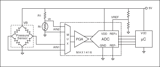
Figure 2. An example of a ratiometric circuit. The output of the pressure sensor, the RTD voltage, and the reference voltage for the ADC are all directly proportional to the supply voltage. This eliminates the need for an absolute voltage reference and simplifies the calculations necessary to determine the actual pressure.
Eliminating the RTD
Silicon-based resistors are highly temperature sensitive, a property that can be exploited by using the bridge resistance as the temperature sensor for the system. This not only reduces cost, but it also yields better results because it eliminates any temperature gradient that may have existed between the RTD and the stress-sensitive bridge. As mentioned previously, absolute accuracy of the temperature measurement is not important as long as the temperature measurement is repeatable and unique. The requirement for uniqueness limits this temperature-sensing method to bridges whose impedance remains constant as pressure is applied. Fortunately, most silicon sensors use a fully active bridge that meets this requirement.
Figure 3 is a circuit where a temperature-dependent voltage is created by placing a resistor (R1) in series with the low-voltage side of the bridge. Adding this resistor reduces the voltage across the bridge and hence its output. This is generally not a large voltage reduction, but it may be enough to require an increase in gain or a decrease in the reference voltage. Equation 8 can be used to calculate a conservative value of R1. It works well when R1 < RB/2, which will be true for most applications.
R1 = (RB × VRES)/(VDD × TCR × TRES - 2.5 × VRES)
Where RB is the input resistance of the sensor bridge, VRES is the voltage resolution of the ADC, VDD is the supply voltage, TCR is the temperature coefficient of resistance of the sensor bridge, and TRES is the desired temperature resolution.
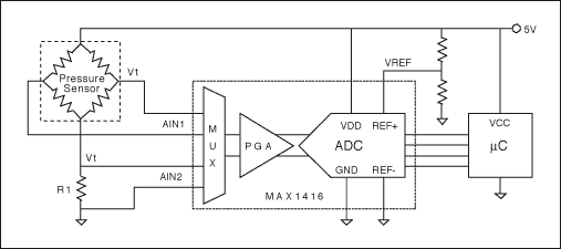
Figure 3. An example of a ratiometric circuit that uses the output of the bridge for pressure measurement and the resistance of the bridge for temperature measurement.
Continuing with the previous example and assuming a desired temperature resolution of 0.05°C, R1 = (4.5kΩ × 30µV/count)/(((5V × 1200ppm/°C × 0.05°C/count) - 2.5) × 30µV/count) = 0.6kΩ. This result is valid since R1 is less than half of RB. In this example, adding R1 will cause a 12% drop in VB. In selecting the converter, however, it was necessary to round up from 17.35 bits to 18 bits of resolution. This increase in resolution more than compensates for the reduction in VB.
As temperature increases, the resistance of the bridge rises causing more voltage to be dropped across it. This change in VB with temperature creates an additional TCS term. Fortunately this term is positive and the inherent TCS of the sensor is negative, so placing a resistor in series with the sensor will actually reduce the uncompensated TCS error. The calibration techniques above are still valid; they just need to compensate a slightly smaller error.
Current-Driven Bridges
A special class of silicon piezoresistive sensors exists that are referred to as constant-current sensors or current-driven sensors. These sensors have been specially processed so that when they are powered by a current source, the sensitivity is constant over temperature (TCS ≈ 0). It is common for current-driven sensors to have additional resistors added that eliminate, or significantly reduce the offset error and OTC error. In essence, analog techniques are being used to calibrate the sensor. This frees the designer from the expensive task of measuring every part over temperature and pressure. The absolute accuracy of these sensors over a wide temperature range is generally not as good as the sensors calibrated digitally. Digital techniques can still be used to improve the performance of these sensors, and temperature information is easily obtained by measuring the voltage across the bridge, which will typically increase at a rate greater than 2000ppm/°C. The circuit in Figure 4 shows a current source powering the bridge. The same voltage reference used to establish a constant current also supplies the reference voltage for the ADC.
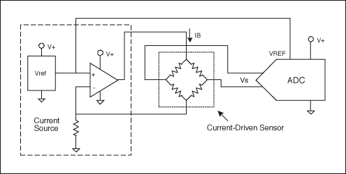
Figure 4. This circuit uses a current driven sensor powered by a conventional current source.
Eliminating the Current Source
Understanding how current-driven sensors compensate for STC allows the circuit in Figure 5 to achieve the same results as the circuit in Figure 4 without including a current source. Current-driven sensors still have an excitation voltage (VB), however, VB is not fixed by a voltage supply. VB is determined by the bridge's resistance and the current through the bridge. As mentioned earlier, silicon resistors have a positive temperature coefficient. This causes VB to increase with temperature when the bridge is powered from a current source. If the bridge's TCR is equal in magnitude and opposite in sign to TCS, then VB will increase with temperature at the right rate to compensate for decreasing sensitivity, and TCS will be near zero over a limited temperature range.
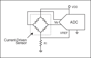
Figure 5. Circuit uses a current-driven sensor, but does not require a current source or a voltage reference.
An equation for the ADC's output in the circuit in Figure 4 can be obtained by starting with Equation 7 and replacing VB with IB times RB. This results in Equation 9, where RB is the input resistance of the bridge and IB is the current through the bridge.
D = (IB × RB/VREF) × ƒ(p,t) × FS × K
The circuit shown in Figure 5 can provide the same performance as the circuit in Figure 4, but without using a current source or voltage reference. This can be shown by comparing the output of the two circuits. The output of the ADC in Figure 5 is found by starting with Equation 7 and substituting the appropriate equations for VB and VREF. This results in Equation 10.
Repeat of Equation 7: D = (VB/VREF) × ƒ(p,t) × FS × K
In the circuit in Figure 5, VB = VDD × RB/(R1 + RB)
And VREF = VDD × R1/(R1 + RB)
Substituting these into Equation 7 yields Equation 10.
D = (RB/R1) × ƒ(p,t) × FS × K
If R1 is selected to equal VREF/IB, then Equations 9 and 10 are identical, which, in turn, shows that the circuit in Figure 5 provides the same results as the circuit in Figure 4. For identical results, R1 must equal VREF/IB, but this is not a requirement to achieve proper temperature compensation. As long as RB is multiplied by a temperature-independent constant, temperature compensation will be achieved. The value of R1 can be selected to best fit the system requirements.
When using the circuit in Figure 5, it is important to remember that the ADC's reference voltage changes with temperature. This makes the ADC unsuitable for monitoring other system voltages. In fact, if a temperature-sensitive measurement is needed for additional compensation, it can be obtained by using an additional ADC channel to measure the supply voltage. Also, when using the circuit in Figure 5, care should also be taken to ensure that VREF is within the specified range for the ADC.
Conclusion
The relatively large output of silicon piezoresistive strain gauges allows them to interface directly with low-cost, high-resolution, sigma-delta ADCs. This eliminates the cost and errors associated with amplification and level-shifting circuits. In addition, the thermal properties of these strain gauges and ratiometric characteristics of the ADC can be used to significantly reduce the complexity of highly accurate circuits.
{{modalTitle}}
{{modalDescription}}
{{dropdownTitle}}
- {{defaultSelectedText}} {{#each projectNames}}
- {{name}} {{/each}} {{#if newProjectText}}
-
 {{newProjectText}}
{{/if}}
{{newProjectText}}
{{/if}}
{{newProjectTitle}}
{{projectNameErrorText}}
Latest Media 21


