Process High-Voltage Input Levels into a Low-Voltage ADC Without Losing Much SNR
Abstract
It is often difficult to find an analog-to-digital converter (ADC) that aligns with the analog input range, but also has the appropriate number of inputs, the needed size, and the correct sample speed. Especially for system designers working with wide voltage swings, there is a concern that scaling down the input signal to drive an ADC's full-scale range can significantly degrade the signal-to-noise ratio (SNR). This application note discusses what affects this SNR loss, how it can be quantified, and more importantly, how it can be minimized.
A similar version of this article appeared on Selezione di Elettronica, September 2012.
A typical misconception when designing with an analog-to-digital converter (ADC) is that scaling down the input signal to drive an ADC's full-scale range will significantly degrade the signal-to-noise ratio (SNR). This is especially a concern for system designers who are working with wide voltage swings. Compounding the issue, there is also a much wider offering of ADCs for the low-voltage supply (5V or less) than for higher voltage supplies. Higher supplies often lend to higher power consumption and board complexity, needing for instance, more decoupling capacitors. This application note discusses what affects the SNR loss introduced by scaling, how it can be quantified, and more importantly, how it can be minimized.
Many signals coming out of a sensor or system are high voltage and bipolar; for instance ±10V is widely used. However, there are simple ways to drive this signal through an ADC, and integrated high-voltage ADC solutions are available that can handle such large full-scale inputs without losing SNR. These solutions usually need extra high-voltage supplies to accommodate the input range and dissipate a fairly large amount of power (Figure 1). These high-voltage ADCs also narrow the range of usable signal conditioning (op amp) solutions. If signals need to be multiplexed with a combination of high-voltage and low-voltage inputs, the implementation could become quite costly (Figure 2).

Figure 1. The MX574A high-voltage ADC accommodates large input signals at the expense of higher power consumption. To implement this solution, both ±15V and +5V supplies are usually needed.
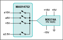
Figure 2. A multiplexed bipolar high-voltage ADC system.
You can also use an input amplifier to perform the signal scaling to drive the low-voltage ADC's full input range. This signal-conditioning circuitry can be connected to a single multiplex input (see Figure 3), so all the signals cover the range of the ADC.
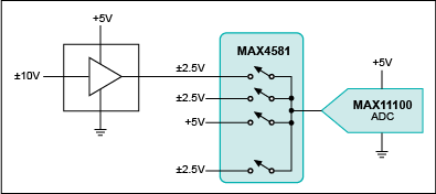
Figure 3. A high-voltage multiplexed system using a single MAX11100 low-voltage ADC.
When an amplifier is used to perform the signal-voltage scaling, the noise is referred back to the input of the amplifier. There are two main sources of noise at this point: the input-referred noise of the amplifier itself and the scale-down input-referred noise of the ADC. These two sources of noise combine in a quadratic manner. Furthermore, the noise of the amplifier is filtered by the input bandwidth of the ADC and by the antialiasing filter present between the amplifier and the ADC's input. See Figure 4.
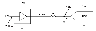
Figure 4. A scaling amplifier introduces noise, but the noise is filtered by the RC and input network of the ADC.
The equation for the system SNR (at the input of the amplifier) becomes:
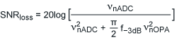
Where:
 nADC = input RMS noise of the ADC
nOPA = input-referred noise of the amp (input-referred X-scale factor)
f-3dB = single pole -3dB frequency
For a given full-scale range of the ADC, input-referred noise for the ADC, and a scaling factor for the amplifier, there are two variables that affect the target SNR loss degradation: filter-cutoff frequency and amplifier input-referred noise.
If the signal source has low-frequency content, the filter can be designed so that the amplifier can tolerate a larger amount of input noise (higher input noise usually is associated with lower power consumption and lower cost). If the ADC limits the bandwidth of the system, the amplifier needs to have enough low input-referred noise to achieve the tolerated SNR loss degradation.
As an example, given a ±10V input signal and a 5VP-P full-scale range ADC with a 92dB SNR, the scaling factor (input to full-scale range) is 4. The input-referred noise of the ADC from the data sheet is 44.4nVRMS. Assuming a filter with a 10kHz cutoff frequency and an amplifier with 10nV/√Hz of input-referred noise, the loss in SNR becomes:
SNR(loss)= 0.035dB
If the filter is not present and the ADC bandwidth is (for instance) 10MHz, the new input-referred noise required to achieve the same SNR loss becomes 0.3nV/√Hz, which is quite stringent.
For the same 10MHz bandwidth in the ADC, if we allow for SNR(loss) = 0.5dB, the noise requirement on the amplifier becomes 4nV/√Hz, which is easier to achieve.
More integrated and highly flexible solutions exist that allow users to input different signal ranges at an input multiplex, program the gain per each input, while doing the scanning and optimize SNR. For example, Analog Devices offers the MAX1300 family of 16-/14-bit ADCs that offer up to 8 input signals, as shown in Figure 5. The MAX1300 accepts bipolar input signals of up to ±12V while using a single 5V power supply, thus reducing external components, power supplies, and board space.

Figure 5. The MAX1300 ADC with programmable input ranges (including bipolar with single supply), programmable gain per sample, and internal reference.
Another flexible system is the MAX11131, a 12-bit, 16-channel, 3Msps ADC. The device has SampleSet™ technology, a user-programmable analog input channel sequencer, which allows for up to 256 arbitrary programmed scanning sequences (Figure 6). SampleSet technology also allows for asymmetrically breaking the input bandwidth, giving system flexibility to handle high- and low-frequency content signals on different channels.
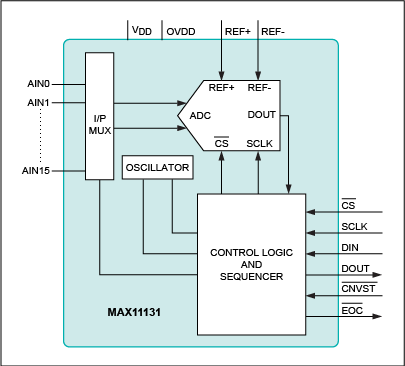
Figure 6. Functional diagram of the MAX11131, a 3Msps, 12-bit, 16-channel ADC with flexible SampleSet multiplex sequencing.
In conclusion, adding a scaling amplifier to convert a high-voltage signal into a full-range low-voltage ADC is quite achievable, given a system bandwidth and tolerable SNR loss. The solution could render a very cost-effective system when multiple-level signals are fed into a multiplexed low-voltage ADC. Analog Devices offers a wide range of data-converter solutions with leadership performance in 16 and 24 bits, as well as integrated filters for antialiasing.
Related to this Article
Products
PRODUCTION
24-/16-Bit, 4-Channel, Simultaneous-Sampling, Cascadable, Sigma-Delta ADCs
PRODUCTION
24-/16-Bit, 4-Channel, Simultaneous-Sampling, Cascadable, Sigma-Delta ADCs
PRODUCTION
24-Bit, Single-Channel, Ultra-Low Power, Delta-Sigma ADCs with GPIO
Product Categories
{{modalTitle}}
{{modalDescription}}
{{dropdownTitle}}
- {{defaultSelectedText}} {{#each projectNames}}
- {{name}} {{/each}} {{#if newProjectText}}
-
 {{newProjectText}}
{{/if}}
{{newProjectText}}
{{/if}}
{{newProjectTitle}}
{{projectNameErrorText}}
Latest Media 21


