Design Trade-offs of Using Precision SAR and Sigma-Delta Converters for Multiplexed Data Acquisition Systems
Design Trade-offs of Using Precision SAR and Sigma-Delta Converters for Multiplexed Data Acquisition Systems
Apr 1 2016
Multiplexed data acquisition systems (DAS) utilized in industrial process control, portable medical devices, and automated test equipment need increased channel density where the user wants to measure the signals from multiple sensors and monitor and scan many input channels into a single ADC or several ADCs. The overall benefit of multiplexing is fewer numbers of ADCs per channel required, saving print circuit board (PCB) space, power, and cost. Some systems in automated test equipment and power line monitoring applications demand dedicated track and hold amplifier and ADC on a per channel basis for simultaneously sampling the inputs to obtain increased sampling rate per channel, and to preserve the phase information at the expense of additional PCB area and power. System designers make trade-offs based on performance, power, size, and cost requirements in their end application. They select one of the converter architectures and topologies and implement their signal chain using either a discrete or integrated components available in the market. Figure 1 shows a simplified block diagram of multiplexed DAS that monitor and sequentially sample various sensor types. Sometimes signal chains utilize either a buffer amplifier or a programmable gain amplifier between the multiplexer and ADC.


Figure 1. Typical multiplexed data acquisition system.
A small voltage glitch or kickback occurs at the multiplexer input when it switches channels. This kickback is a function of the turn-on and turn-off times, on resistance, and load capacitance of the multiplexer. Large switches with low on resistance typically result in a large output capacitance that must be charged to a new voltage each time the input is switched. If the output doesn’t settle to a new voltage, crosstalk error will occur. Therefore, the multiplexer’s bandwidth must be sufficient and a buffer amplifier or large capacitors must be used at the multiplexer input to settle a full-scale step. In addition, the leakage current flowing through the on resistance will introduce a gain error, so both should be kept small.
SAR vs. Σ-Δ ADC Architecture
Figure 2 shows the basic converter architecture of a successive approximation register (SAR) based on the charge redistribution capacitor digital-to-analog converter (DAC) array. It samples the input signal once at each convert start edge, compares the bit on each clock edge, and adjusts output of the digital-to-analog converter through control logic until that output very closely matches the analog input. So it requires N-number of clock cycles from an independent external clock to implement a single N-bit conversion in an iterative manner.

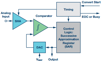
Figure 2. Basic SAR ADC architecture.

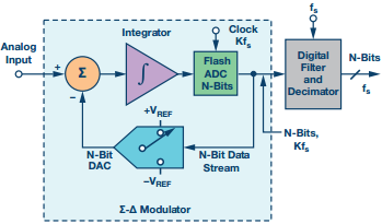
Figure 3. Basic Σ-Δ ADC architecture.
The internal comparator noise and DAC linearity determines the accuracy of SAR ADC conversion, whereas the settling time (switching) of the integrator in the modulator determines the accuracy of the Σ-Δ ADC conversion. One of the challenges with the SAR ADC is that the driver amplifier needs to settle switching transient currents injected on its analog input during the acquisition time between the end of one conversion and the start of the next conversion.
The input bandwidth of SAR ADCs (tens of MHz) is higher than the sampling frequency. The desired input signal bandwidth is typically within tens to hundreds of kHz—so the antialiasing is required to filter out unwanted aliases folding back to bandwidth of interest. In the case of Σ-Δ ADC, the desired input signal bandwidth is usually from dc to a few kHz, and the input bandwidth of the digital filter is lower than the sampling frequency of the modulator, so it relaxes the antialiasing requirements. The digital filter removes the noise outside the bandwidth of interest and the decimator then reduces the output data rate back to the Nyquist rate.
Multiplexed Applications Challenges
Precision SAR ADCs are popular in many applications due to their ease of use, low power, small package, and low latency that simplifies fast channel switching in multiplexed DAS. Precision Σ-Δ ADCs are popular in industrial and audio applications for out of band rejection and its ability to reject the 1/f noise content close to dc (50 Hz/60 Hz) when chopping is implemented. In this case, high resolution is traded for the sampling rate of the ADC.
The SAR ADC is inherently asynchronous, enabling fast control loop design with nearly zero latency or pipeline delay associated with the conversions and fast response to step input near full scale—therefore, it’s a popular choice for many multiplexed applications. Whereas, the Σ-Δ converter architecture is conventionally monotonic (meaning it can convert at any one point in time) and uses integrated modulator for oversampling and digital decimation filtering that requires a global internal or external clock source to synchronize all the internal blocks—resulting in a nonzero cycle latency or settling time issue. Some of the systems also rely on having uniformity across multiple channels in the digitization process with low latency enabling multiplexing for easier and faster channel switching using SAR ADCs. Despite the latency (group delay) of digital filter, the Σ-Δ ADCs are often popular for multiplexing various sensor types such as temperature, pressure, or load cells to acquire small voltage changes at a slow output data rate, such as process control. This is mainly due to its high resolution, accuracy, noise, and dynamic range performance, whereas SAR ADCs usually require low-pass filtering or buffering on each channel, which adds complexity in terms of space and cost.
The higher throughput rate of some precision SAR ADCs allow multiple channels to be multiplexed at fast scan rates for the digitizing process so fewer number of ADCs are required, saving PCB area and cost. The output data rate at which precision Σ-Δ ADCs can multiplex is limited by the settling time of the digital filter type, which limits its ability to settle fast full-scale transitions of multiplexer channels. The settling time also varies depending on the type of the digital filter used. A user must wait the full settling time of the digital filter before a valid conversion result can be achieved and then the channel can be switched to the next channel. Some of the Σ-Δ ADCs with inbuilt sinc (sinx/x) digital filters allow a single cycle settling or zero latency by masking the internal digital filter results and output the data results fully settled within the first conversion or before a new sampling period is initiated. These ADCs’w output data rate is always less than their fully settled latency time.
The common issues faced by both types of precision ADCs in the multiplexed applications are bandwidth, settling time, and input range requirements. In a multiplexed DAS, when the input channel is switched to the next channel, one of the key challenges is that ADC must be able to support a large voltage amplitude step change and fast transition, even for dc type signals, because the input step could go from negative full-scale voltage (sometimes ground) to positive full-scale voltage or vice versa. In other words, a large voltage step between the input channels is generated in a small amount of time and the ADC input must be able to settle this large voltage step. This puts an additional burden on the ADC driver and a large signal bandwidth of the ADC driver becomes a critical spec for the choice of ADC driver in this case. With a large amplitude step, nonlinear effects appear and the slew rate and output current characteristics limit the ADC driver capabilities and output response. The multiplexer channel switching must be synchronized with ADC conversion pin and it should switch to the next channel after a small switching delay (tens of ns) from the initiation of conversion to allow maximum time to settle the selected channel. To guarantee performance at maximum throughput, all of the components in the multiplexed system must fully settle at the ADC input between the time that the multiplexer switches and next conversion begins.
Integrated and Discrete Multiplexed Precision DAS Solutions
There are two types of precision DAS solutions available for multiplexed applications in the market today depending on the customer’s needs: integrated and discrete components. The benefit of a discrete multiplexed solution appears in terms of flexibility in the selection of appropriate signal conditioning components based on their performance requirements. The users still have to worry about complex design issues related to the channel switching, sequencing, and settling time. One could also argue that users have the flexibility of when they can switch the multiplexer input channels and do the external calibration to calibrate out errors—but it will likely increase their boards’ sizes and costs at the expense of performance and flexibility. Some customers also prefer to do their own custom digital filtering on the FPGAs rather than use those that are available on chip for their flexibly.
If the customers use integrated multiplexed-based solutions, they don’t need to worry about channel switching, sequencing, and settling time issues. In addition, this approach could offer per channel configurations, with different input ranges and error calibration options. In this case, the customers have less flexibility on the signal conditioning, but this approach could simplify their designs and save them area and bill of materials costs, while offering adequate performance. Some of the highly integrated SAR and Σ-Δ ADCs available today alleviate many of the challenges associated with designing a precision DAS. These ICs eliminate the necessity to buffer, level shift, amplify, attenuate, or otherwise condition the input signal. They also eliminate the concerns regarding common-mode rejection, noise, channel switching, sequencing, and settling time.
System designers should consider design pros and cons presented here when selecting either SAR or Σ-Δ converter architecture based on performance, power, size, and cost requirements for their multiplexed data acquisition system.
About the Authors
Maithil Pachchigar is a systems application engineer in the Industrial and Multimarkets Business Unit at Analog Devices, Inc., in Wilmington, MA. Since joining ADI in 2010, he has been focused on the precision signal chain...
Related to this Article
Industry Solutions
{{modalTitle}}
{{modalDescription}}
{{dropdownTitle}}
- {{defaultSelectedText}} {{#each projectNames}}
- {{name}} {{/each}} {{#if newProjectText}}
-
 {{newProjectText}}
{{/if}}
{{newProjectText}}
{{/if}}
{{newProjectTitle}}
{{projectNameErrorText}}
Latest Media 21


