Polyimide Film Uses for Digital Isolators
Abstract
Digital isolators provide compelling benefits over legacy optocouplers in terms of high speed, low power consumption, high reliability, small size, high integration, and ease of use. Billions of digital isolators using microtransformers have been widely adopted in many markets, including automotive, industry automation, medical, and energy. What are essential for the high voltage performance of these digital isolators are polyimide films deposited in between the top spiral winding and bottom spiral winding for the stacked winding transformers. In this article, digital isolator construction using polyimide films as isolation layers will be reviewed. To meet various safety standards such as UL and VDE, digital isolators need to satisfy various high voltage performances, such as short duration withstand voltage, surge voltage, and working voltage. Polyimide aging behavior under various high voltage waveforms such as ac or dc was studied, and isolator working voltage is extrapolated through a polyimide lifetime model. Structural improvements to improve polyimide high voltage lifetime will also be discussed.
Introduction
Isolation between circuit components is typically required for safety and/or data integrity considerations. For example, isolation protects sensitive circuit components and human interface on the system side from dangerous voltage levels present on the field side, where more robust components such as sensors and actuators reside. Isolation can also eliminate common-mode noises or ground loops that affect data acquisition accuracy. While optocouplers have provided isolation for decades, they present significant limitations in terms of low speed, high power consumption, and limited reliability. Their low bandwidth and long propagation delay present significant challenges in meeting the ever-increasing speed requirements for many isolated field bus communications such as RS-485 in industry automation systems.
Their high power consumption due to their LED puts a significant constraint on the overall system power budget in power limited industry systems such as process control 4 mA to 20 mA systems. As the current transfer ratio for optocouplers degrades over time, especially at high temperatures, it fails to meet the reliability needs for demanding applications such as automotive.
Digital isolators remove the penalties associated with isolation and they provide compelling advantages over optocouplers in terms of high speed, low power consumption, high reliability, small size, high integration, and ease of use. Digital isolators using microtransformers1,2 allow for the integration of multiple transformers and other necessary circuit functions. The stacked spirals used in digital isolators provide tight magnetic coupling between the top coil and bottom coil, and very little coupling between spirals side by side. This enables multiple channel integration with little interference between the channels. The magnetic coupling between the top spiral and bottom spiral depends only on the size and separation. Unlike the current transfer ratio for the optocouplers, it does not degrade over time, which leads to the high reliability for these digital isolators based on transformers. These transformers have a self-resonant frequency from a few hundred MHz to a few GHz and they can be used to realize digital isolators from 150 Mbps to 600 Mbps. With a high quality factor well over 10 for these transformers, the power consumption for these digital isolators is orders of magnitude lower than those of optocouplers.
The optocouplers shown in Figure 1 rely on a few mm thick molding compound between the LED die and photodiode die to achieve isolation. For the transformer-based digital isolators shown in Figure 2, isolation performance is mainly limited by 20 μm to 40 μm thick polyimide layers sandwiched between the top and bottom coils of the chip scale microtransformers. We will review the detailed construction of these isolators, deposition methods for these polyimide films, characterization of the polyimide films, high voltage performance, and aging behavior for the digital isolators.

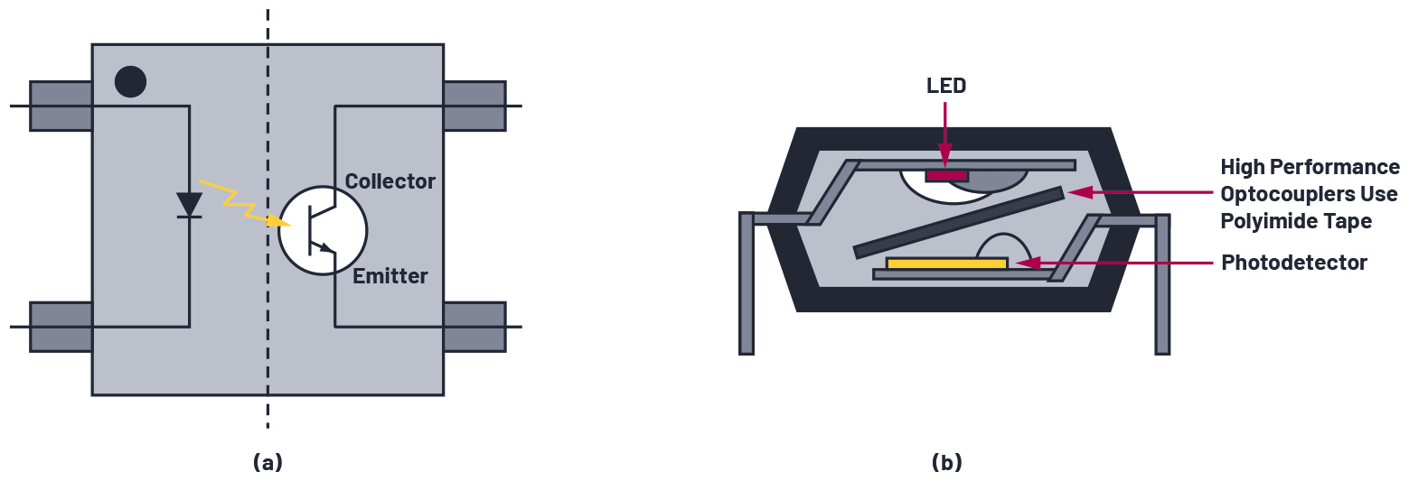
Figure 1. (a) An optocoupler schematic and (b) an optocoupler package cross-section.

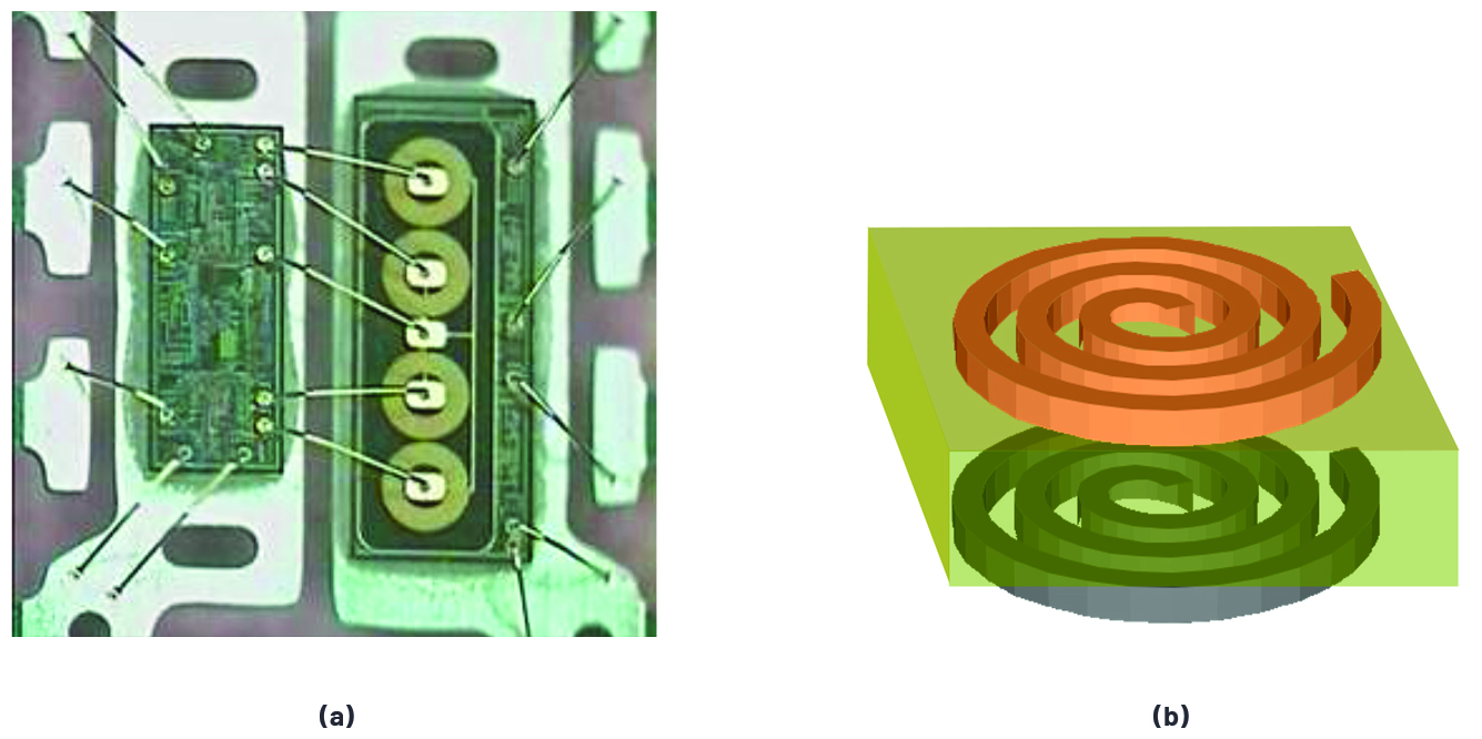
Figure 2. (a) A digital isolator in a plastic package and (b) a transformer cross-section.
Polyimide Film Applications for Digital Isolators
Polyimide is a polymer composed of imide monomers. Polyimide is used as the insulating material in many digital isolators for a number of reasons, including excellent breakdown strength, thermal and mechanical stability, chemical resistance, ESD performance, and relatively low permittivity. Besides good high voltage performance, polyimide has excellent ESD performance that is capable of handling EOS and ESD events exceeding 15 kV.3 During energy limited ESD events, the polyimide polymer absorbs some of the charge to form stable radicals that interrupt the avalanche process and bleeds away some of the charge. Other dielectric materials such as oxide typically do not have this ESD tolerant characteristic and may go into avalanche once the ESD level exceeds the dielectric strength, even if the ESD energy is low. The polyimide also has high thermal stability, with a weight loss temperature over 500°C and a glass transition temperature of about 260°C. The polyimide also has high mechanical stability with a tensile strength over 120 MPa and a high elastic elongation over 30%. In spite of its high elongation, polyimide does not deform easily because the Young’s modulus is about 3.3 GPa.
The polyimide has excellent chemical resistance, which is one reason it has been widely used for insulation coatings for high voltage cables. Polyimide films can be coated on the semiconductor wafer substrates and high chemical resistance also helps to facilitate IC processing on top of polyimide layers, such as the Au plating used to create iCoupler® transformer coils. Lastly, the thick polyimide films, with a dielectric constant of 3.3, work well with the small diameter Au transformer coils to minimize capacitance across the isolation barrier. Most iCoupler products exhibit less than 2.5 pF capacitance between input and output. Because of these characteristics, polyimide is increasingly used in microelectronics applications, and it is an excellent choice as insulating material for the iCoupler high voltage digital isolators.
Digital Isolator Construction and Fabrication
There are three major components for a digital isolator: isolation barrier coupling element, insulation material, and signaling schemes through the isolation barrier. Insulation material is used for the isolation barrier to achieve a certain isolation rating, and the isolation rating mainly depends on the dielectric strength and its thickness. There are two main types of dielectric materials: organic, such as polyimide, and inorganic, such as silicon dioxide or silicon nitride. Both oxide and nitride have an excellent dielectric strength of 700 V/μm to 1000 V/μm. However, they have inherent high stress to prevent film thicker than 15 μm to 20 μm to be reliably formed on a large scale modern IC wafer. The other limitation to organic films is that they are susceptible to ESD; a tiny amount of voltage overstress will lead to catastrophic avalanche breakdown. Organic films such as polyimide consist of long C-H chains, and a small ESD event with limited energy may break some local C-H links without compromising material structural integrity, and they tend to be much more ESD tolerant. Polyimide does not compare favorably to oxide or nitride in terms of dielectric strength—around 600 V/µm to 800 V/µm. However, with inherent low film stress, much thicker polyimide layers as much as 40 µm to 60 µm can be economically formed. 30 µm polyimide films provide withstand voltages in the 18 kV to 24 kV range, which is better than 20 µm oxide with withstand voltages in the 14 kV to 20 kV range. For applications with robust ESD performance and high voltage withstand capability against impulse voltages such as those present during lightning strikes, polyimide-based isolators provide the most robust choice.
Commercial polyimide films are available in photoresist form that are deposited on wafers with well controlled thicknesses and then patterned with standard photolithography processes. Here is the process flow shown in Figure 3 for the isolation transformers used for the digital isolators. A CMOS wafer with its top metal layer forming the bottom coil is spin coated with the first photosensitive polyimide and the polyimide layer is patterned through photolithography. The polyimide is then thermally cured to achieve high structural quality. The top coil layer is plated, after which a second polyimide layer is coated, patterned, and cured to form the encapsulation for the top coil. Because deposited polyimide films are free of voids, as shown in Figure 4, and do not suffer from corona discharge, the transformer devices also exhibit good aging behavior and work well under continuous ac voltages and dc voltages.


Figure 3. An isolation transformer process flow.


Figure 4. A cross-section of the fabricated isolation transformer.
High Voltage Performances for Digital Isolators
Isolation rating is defined by the maximum withstand voltage with 1 minute duration per UL 1577. For the production test, the digital isolators were tested for 1 second at 120% of their rated voltage. For 2.5 kV rms 1 min rated digital isolators, the equivalent production test was 3 kV rms for 1 second. For practical applications, there are two important high voltage performance parameters. One is the maximum working voltage where the insulation needs to be intact over the lifetime of continuous operation, ac or dc. For example, per VDE 0884-11, the lifetime for isolators with a reinforced isolation at 120% of the rated voltage needs to be greater than 37.5 years at a 1 ppm failure rate. As an example, if the rated working voltage for a reinforced digital isolator is 1 kV rms, its lifetime at 1.2 kV rms needs to be greater than 37.5 years at a 1 ppm failure rate. Similarly, the lifetime for isolators with basic insulation at 120% of the rated voltage needs to be better than 26 years with 1000 ppm failure. The other important application specification is the maximum transient isolation voltage where the part needs to survive. Transient test waveforms may vary, and an example waveform per EN 60747-5-5 or IEC 61010-1 is shown in Figure 5. Its rise time from 10% to 90% is about 1.2 μs while the falling time from peak to 50% is 50 μs. This intends to simulate the lightning condition, so it is important for isolators to have robust surge performance to be robust in the field. ESD tolerance is an important attribute for semiconductor devices, and high surge performance also imply excellent ESD performance.


Figure 5. IEC 61010-1 surge test waveform.
Polyimide Films Characterization
Figure 6 shows the main intrinsic electrical properties of spin-coated polyimide films measured at wafer level. On one hand, the dc bulk conductivity of polyimide shows very low values around 10-16 S/m over an applied electric field range up to 40 V/µm, but remaining quite low at least up to 150 V/µm. On the other hand, the ac breakdown field of the polyimide films exhibits a minimum value of 450 V rms/µm at 60 Hz. All these make spin-coated polyimide films very good insulating materials for reliable digital isolator applications.

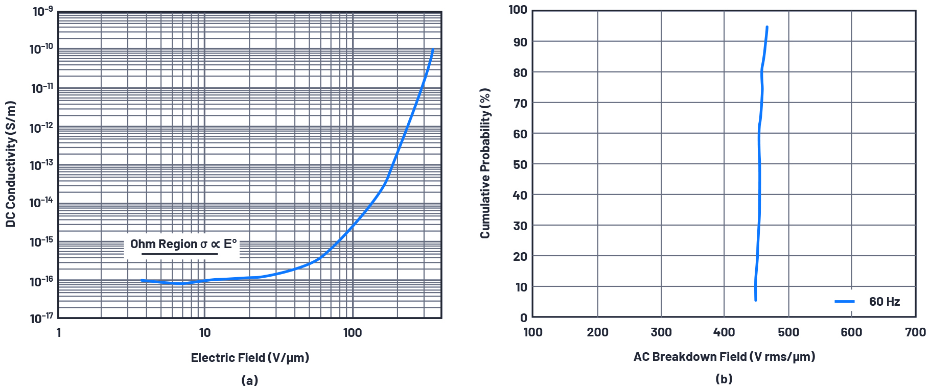
Figure 7 shows the surge performance for isolators with 30 μm thick polyimide films. These isolators will pass surge tests up to 18 kV, and the first failure voltage is 19 kV for a negative pulse and the first failure voltage is 20 kV for a positive pulse.


Figure 7. Surge performance for isolators with polyimide films 30 μm thick.
Polyimide Films Aging
Polyimide lifetime is studied through a high voltage endurance test. Any insulator, given sufficient time and voltage, will break down. An example setup is shown in Figure 8. Multiple parts are connected electrically in parallel, and multiple groups of parts are stressed in different high voltages from high voltage power supplies, and a switch/measurement unit such as Agilent 34980 together with a PC can be used to monitor the time the number of units have broken down. This can be a time consuming process where it can take days to months for the units to break down.

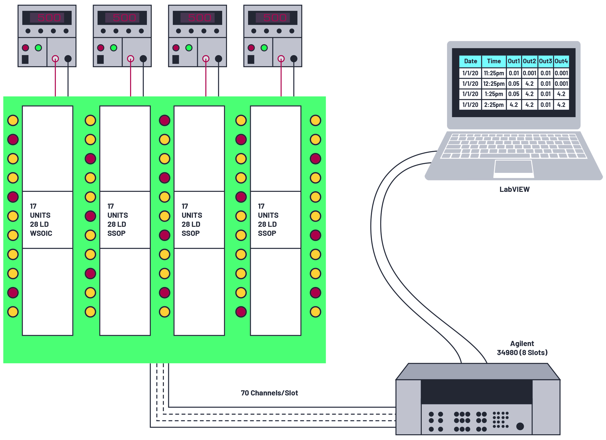
Figure 8. Experimental setup for high voltage endurance test.
The distributions for the time to failure can be analyzed through Weibull plots, as shown in Figure 9. Groups of 16 parts were stressed at six different voltages, where each group forms a fairly decent Weibull distribution. Through Weibull plots, mean time to failure (MTTF) or time to failure at certain failure rate such as 1 ppm can be estimated. Obviously time to failure at high voltages takes much less time compared to that at low voltages. Per VDE 0884-11, the smallest to the largest MTTF need to span at least two orders of magnitude and, at the lowest test voltage, the 63% time to failure needs to be longer than 1E7 seconds or about 116 days. Figure 9 shows that the data sets generated at these six voltages meet these requirements.


To extrapolate working voltage, time to failure is plotted against stress voltages. For basic insulation, working voltage is determined from the voltage with 20% derating where time to failure or lifetime at 1000 ppm is greater than 24 years. Similarly, for reinforced insulation, working voltage is determined from the voltage with 20% derating where the lifetime at 1 ppm is greater than 30 years
The dominant breakdown mechanism is through charge injections as a result of the direct electron impact from the electrodes to the polyimide surface regions. The breakdown process begins as charges are injected into polyimide surface under HVac conditions. The charges can become trapped in some local trapping sites at the surface. Once trapped, energy will be released, which will cause local mechanical tension because of stored electrostatic energy. Through a quantum activation process, this tension will eventually cause local free volumes (voids or micro-cracks) that act as more local trapping sites. If the HVac remains long enough, this process will lead to the continued degradation of insulation and eventually electrical punch-through.
Through thermodynamic analysis, the lifetime, L,4 can be expressed as shown in Equation 1:
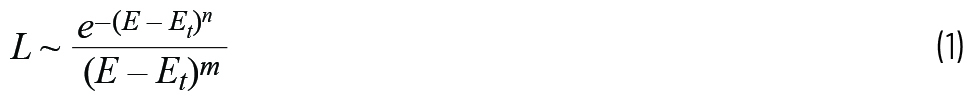
Where Et is the threshold field where no charge injection will happen, and m and n are scaling constants.
The HVac endurance data of iCoupler devices was analyzed according to the procedure specified by ANSI/IEEE std 930-1987, the “IEEE Guide for the Statistical Analysis of Electrical Insulation Voltage Endurance Data,” and it is observed to follow.
This phenomenological fit, as shown in Equation 2, was used to find the worst-case lifetime because it assumes no threshold field as specified by the thermodynamic model. The duration of the HV test becomes prohibitively long if we try to measure the threshold field. Equation 2 was used to model the time to failure for Figure 10. As you can see, the model fits the data rather well.


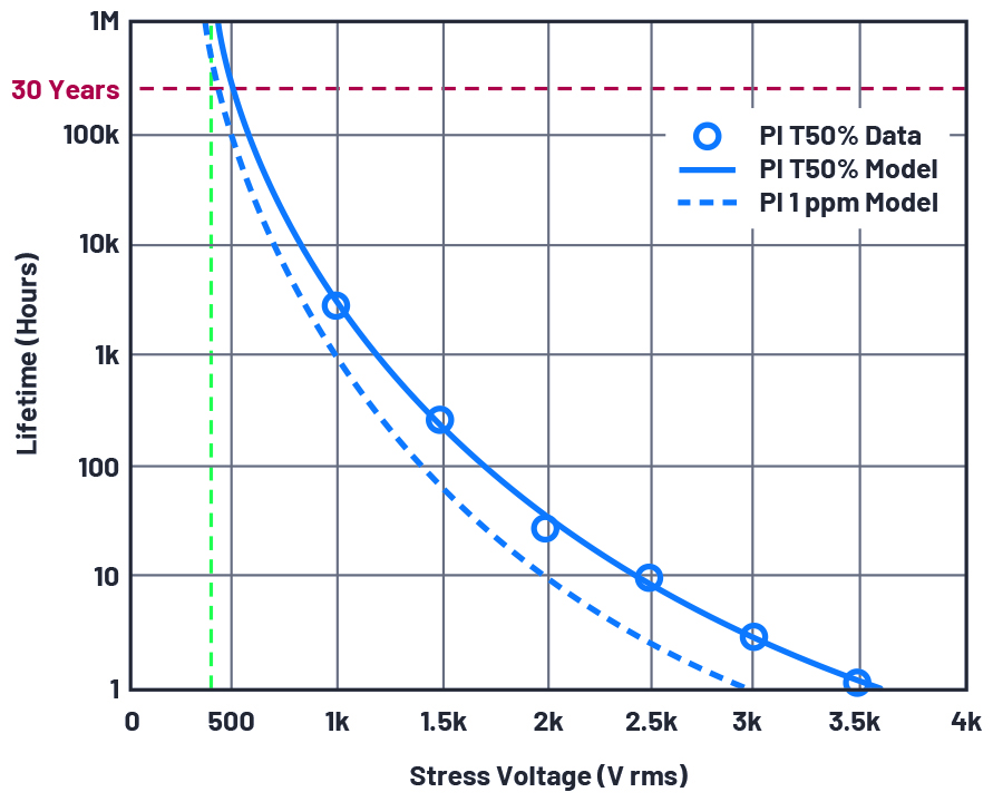
Figure 10. Time to failure plot for isolators with 20 μm thick polyimide.
We also observed that the lifetime of iCoupler devices under dc or unipolar ac is much longer compared to that under bipolar ac; it is at least two orders of magnitude higher. For unipolar waveforms, the trapped charges tend to form an internal field barrier region around the electrodes that prevents further injection of charge into the polyimide, as shown in Figure 11. With a bipolar ac waveform, the reverse of field will prevent formation of this steady field barrier, and the trapped regions will keep progressing into the polyimide and eventually lead to the electrical breakdown. SiO2, on the other hand, tends to give worse lifetime for dc or unipolar ac.

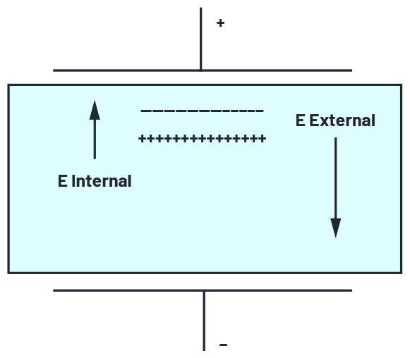
Figure 11. A field barrier region with zero net e-field formed by the trapped charges.
The lifetime shown in Figure 10 is based on worst-case bipolar ac waveforms. HV lifetime is even greater for unipolar ac or dc waveforms. The models described in this article relate to polyimide insulation and have no bearing on isolators that use SiO2 insulators as the primary means for isolation. Likewise, models that predict the HV lifetime of SiO2-based digital isolators have no bearing on polyimide-based isolation systems.
Figure 12 shows how the lifetime for unipolar is compared to that of bipolar for polyimide films. As can be seen, the peak stress voltage for unipolar is about twice that of the peak stress voltage for ac bipolar for the same time to failure. In essence, the lifetime is dependent on the peak-to-peak rather than the peak stress voltage for the polyimide films.


Figure 12. Time to failure comparisons for ac bipolar vs. unipolar.
Polyimide Films Structural Improvements
To improve high voltage endurance for the polyimide, a charge injection barrier can be used as shown in Figure 13.5,6 Preferably, the charge injection barrier will use an oxide or nitride with a large band gap and high dielectric constant. A high dielectric constant will help reduce the electric field close to the electrode, while a large band gap raises the energy barrier for charge injection.

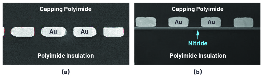
Figure 13. An isolation transformer (a) without and (b) with a nitride charge injection barrier.
To analyze the charge injection for a given isolation system, a band diagram can be drawn, as shown in Figure 14. The four key materials for the isolation system shown in Figure 13 are Au, the top coil material; polyimide, the isolation material between the top coil and bottom coil; oxide, the charge injection barrier; and TiW, the seed layer under the Au. The charge injection from Au or TiW into polyimide or oxide for electrons or holes can be calculated from the band diagram


Figure 14. Band diagram for charge injection.
Figure 15 presents the charging currents over time for polyimide and polyimide with SiN injection barriers measured under 1000 V. The steady state current when the SiN barrier is introduced is reduced by more than 5 times compared to that of polyimide only. This highlights a significant reduction of the charge injection processes that are well known to be responsible for electrical aging with a high electric field.

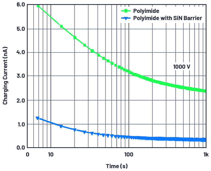
Figure 15. Charging currents comparison for polyimide and polyimide with SiN injection barrier under 1 kV.
Figure 16 presents the time to failure (HVE tests) vs. ac applied voltage from 1 kV rms up to 3.5 kV rms at 60 Hz for isolators with polyimide and polyimide/SiN barriers single die configurations. The lifetime at 50% and the extrapolation at 1 ppm of the dataset are presented. Moreover, for both cases, the extrapolated working voltages at a 30-year lifetime are reported. Digital isolator devices with polyimide insulation exhibits a 400 V rms working voltage while the improved design involving SiN injection barriers shows >900 V rms working voltage at 1 ppm (750 V rms after 20% voltage derating). Based on wafer-level analysis comparison, it is reasonable to attribute the lifetime and working voltage improvements to the SiN injection barriers between polyimide and metallic coils. These SiN thin layers, by mitigating bipolar charge injection at the onset of space charge formation, reduce the electrical current, reduce the related thermal effects, and, very likely, extend the lifetime for a given voltage.

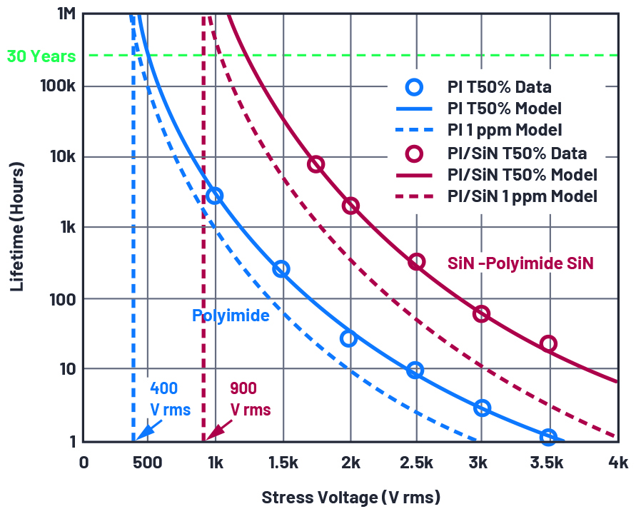
Figure 16. Time-to-failure comparison for polyimide isolators with and without an SiN charge injection barrier.
Conclusion
Polyimide films have excellent high voltage performance from surge voltage to their high voltage endurance. These films have been characterized and the aging behavior can be further enhanced through a charge injection barrier with a large dielectric constant and large band gap. Polyimide film uses for digital isolators are introduced and these polyimide films are excellent candidates for an isolation barrier for digital isolators.
About the Authors
Related to this Article
Industry Solutions
Technology Solutions