Pass Transistor Boosts Current from Negative Linear Regulator
Abstract
The addition of a pass transistor to the circuit of Figure 1 allows the linear regulator (LDO) to deliver more current to the load. A detailed power dissipation analysis is included to assist circuit developers in choosing the proper power rating of each component. Furthermore, lab data shows that the device is stable across temperature, line, and load.
Adding four components to a negative linear regulator (U1 in Figure 1) increases the allowable load current by 60%. Cost for the components is less than $0.17 in 1k quantities.

Figure 1. A pass transistor and associated resistors boosts load current in this negative linear regulator by 60%.
Connecting the SET terminal to ground sets U1's output voltage to -2.5V. U1's maximum load current is 200mA, and the extra components (Q1, R1, R2, and R3) draw another 120mA maximum from the load, producing (without degrading the output regulation) a total maximum load current of 320mA.
R1 reduces the power dissipated in Q1, prevents thermal runaway in Q1, and provides momentary protection against short-circuited outputs. It also prevents oscillation by limiting gain in the Q1 loop. Current flowing through U1 from OUT to VSS produces a voltage drop of VR2 across R2 and R3, and thereby allows Q1 to conduct load current as VR2 approaches the base-to-emitter threshold of Q1. The threshold (VBE) is approximately 0.7V at room temperature.
Choose the values of R1, R2, and R3 to ensure that R2, R3 and Q1 dissipate maximum power at the maximum load current (320mA in this case). At 320mA, U1 conducts 200mA and Q1 conducts 120mA. Component power dissipation at maximum load is as follows:
PR1 = IR1² × R1 = 120mA² × 9.1Ω ≈ 131mW
PQ1 = VQ1 × IQ1 = (VSS - VR1 - VOUT) × IQ1 = (5V - 1.1V - 2.5V) × 120mA ≈ 168mW
PR2 = IR2² × R2 = 100mA² × 18Ω ≈ 180mW
PR3 = IR3² × R3 = 100mA² × 18Ω ≈ 180mW
PU1 = VU1 × IU1 = (VSS - VR2 - VOUT) × IU1 = (5V - 1.8V - 2.5V) × 200mA ≈ 140mW
To provide higher load current, you can easily modify the circuit by increasing the power-dissipation ratings of R1, R2, R3, and Q1. Table 1 details the components shown for 320mA load current. For power dissipation, the circuit board should have ample copper connected to the leads of power-dissipating components. Heat then conducts through the component leads to the circuit board, spreads into the copper areas, and is removed from the board by convection.
| Component |
Manufacturer Part Number Description |
Package | Power Dissipation | Allowable Power Dissipation at +85°C |
| R1 |
KAMAYA, INC. RMC18-9R1JB 9.1Ω ±5% Resistor |
1206 |
250mW derate 4.55mW/°C above +70°C |
181.75mW |
| R2, R3 |
KAMAYA, INC. RMC18-18RJB 18Ω ±5% Resistor |
1206 |
250mW derate 4.55mW/°C above +70°C |
181.75mW |
| Q1 |
Central Semiconductor Corp. CMPT2222A NPN Transistor |
SOT23-3 |
350mW derate 2.8mW/°C above +25°C |
182mW |
| U1 |
Maxim Integrated MAX1735EUK25 200mA Negative LDO |
SOT23-5 |
571mW derate 7.1mW/°C above +70°C |
464.5mW |

Figure 2a.
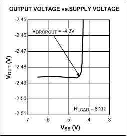
Figure 2b.

Figure 2c.

Figure 2d.

Figure 2e.

Figure 2f.
Figure 2. Curves and waveforms characterize the output of Figure 1: output voltage vs. load current (a), output voltage vs. supply voltage (b), output voltage vs. temperature (c), line transient response (d), load transient response (e), and shutdown response (f).
A similar version of this article appeared in the November 25, 2002 issue of EDN magazine.
Related to this Article
Products
Product Categories
{{modalTitle}}
{{modalDescription}}
{{dropdownTitle}}
- {{defaultSelectedText}} {{#each projectNames}}
- {{name}} {{/each}} {{#if newProjectText}}
-
 {{newProjectText}}
{{/if}}
{{newProjectText}}
{{/if}}
{{newProjectTitle}}
{{projectNameErrorText}}
Latest Media 21


