Over-the-Air Pattern Measurements for a 32-Element Hybrid Beamforming Phased Array
Over-the-Air Pattern Measurements for a 32-Element Hybrid Beamforming Phased Array
Abstract
In this paper we summarize measured receive antenna performance for a commercially available 32-element phased array demonstrator. The demonstrator is configured for hybrid beamforming with eight elements per subarray and four digital channels. The test setup and calibration steps are explained sequentially along with the measured calibration accuracy achieved. Three-dimensional radiation patterns of the antenna array are shown for various electronically steered beam positions including amplitude tapering.
Introduction
The proliferation of phased arrays in both commercial as well as aerospace and defense applications has driven the development of many dedicated integrated circuits (ICs) to enable practical implementations of highly integrated solutions. Several stages of prototyping and development are needed for both hardware validation and software development prior to the transition into a final product. To help streamline phased array product development, complete multichannel demonstrators are becoming commercially available.1,2 As part of the release process, the hardware demonstrators are characterized in a manner to enable performance assessments. This data can be leveraged by system engineers during the architecture definition phase.3,4,5
Here we describe receiver antenna patterns measured on hardware commercially available for full hybrid beamforming phased array characterization. The hardware platform is intended to enable ease of entry into real-time hybrid beamforming signal processing development and save time in the prototyping phases. By characterizing the entire electronic suite ahead of time and in parallel with software development, hardware development becomes a repackaging effort improving overall time to market.
Notable aspects of this platform include:
- The incorporation of the latest commercially available direct sampling C-band digital-to-analog converters (DACs) and analog-to-digital converters (ADCs) that leverage embedded digital signal processing (DSP). The embedded DSP thus offloads traditional FPGA functions into dedicated hardened silicon on chip
- Digital upconverters (DUCs)
- Digital downconverters (DDCs)
- Numerically controlled oscillator (NCO) frequency and phase control
- Incorporates commercially available X-band beamformer ICs (BFICs)
- Independent amplitude and phase control for both transmit and receive
- Integrates BFICs with transmit/receive modules (TRMs) within an X-band lattice spacing
- MATLAB® control enables rapid adoption of full phased array testbeds to evaluate application specific radio signal digital processing
Being able to directly validate ICs in a full system testbed enables the opportunity to validate compatibility of component integration, estimate performance, and to incorporate lessons learned into next-generation ICs.
Hardware Demonstrator Description
A 32-element hybrid beamforming prototype system platform has been developed where the detailed signal chain block diagram is shown in Figure 1.1 The antenna array is a 4 × 8 planar array consisting of microstrip patch antennas. The patch antennas are linear polarized at 45° with equal spacing between elements equal to one-half a wavelength at 10 GHz. The front-end electronics consists of 32 TRMs and eight analog BFICs. Two BFIC outputs combine to produce four 8-element subarrays. The four subarrays connect to a 4-channel microwave up/downconverter. The 4-channel microwave up/downconverter then connects to a digitizer IC that contains four ADCs and four DACs. The ADCs sample at 4 GSPS whereas the DACs sample at 12 GSPS.
The microwave frequencies characterized are from 8 GHz to 12 GHz. The local oscillator (LO) is set to a high-side LO with a fixed IF centered at 4.5 GHz. At this IF frequency, the ADC is sampling in the third Nyquist zone and the DAC is sampling in the first Nyquist zone.
A commercial FPGA board is used for data capture. A MATLAB computer control interface has been developed enabling rapid characterization of simulated waveforms in real hardware. Data analysis is performed with postprocessing in MATLAB.
Test Setup
Radiation pattern measurements are conducted using the MilliBox MBX33 anechoic chamber placed on a 10-foot lab bench.6 The test configuration is presented in a block diagram depiction as detailed in Figure 2a. The antenna array, analog beamforming board, and microwave splitters are mounted on the GIM04 3-axis antenna positioner gimbal using a custom adapter plate shown in Figure 2b. The RF cables are routed to the microwave up/downconverter through the PassThru™ channel of the gimbal where the rest of the signal chain resides below the chamber. The digital control and DC power cables are also routed through the PassThru channel to the FPGA controller and power supply.
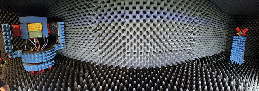
Located in the far-field of the antenna array is a X-band horn antenna connected to a signal generator located below the anechoic chamber. With a minimum far-field of approximately 1 meter, the transmitting horn antenna is located at 1.55 meters. The controller PC controls the hybrid beamforming system platform, signal generator, and gimbal positioner all within MATLAB to conduct the calibration and measurements presented herein.


For receive radiation patterns, the horn antenna radiates a continuous wave signal towards the array. The transmit power from the signal generator is adjusted for the array to receive a nominal power in the range of –5 dBFS to –10 dBFS when all elements are calibrated in both amplitude and phase. The peak FFT magnitude is recorded for each angular position as the antenna array is mechanically rotated in 1° steps from ±90° in both the azimuth and elevation planes. The radiation patterns are created by plotting the peak FFT value vs. the angular position of the antenna array.

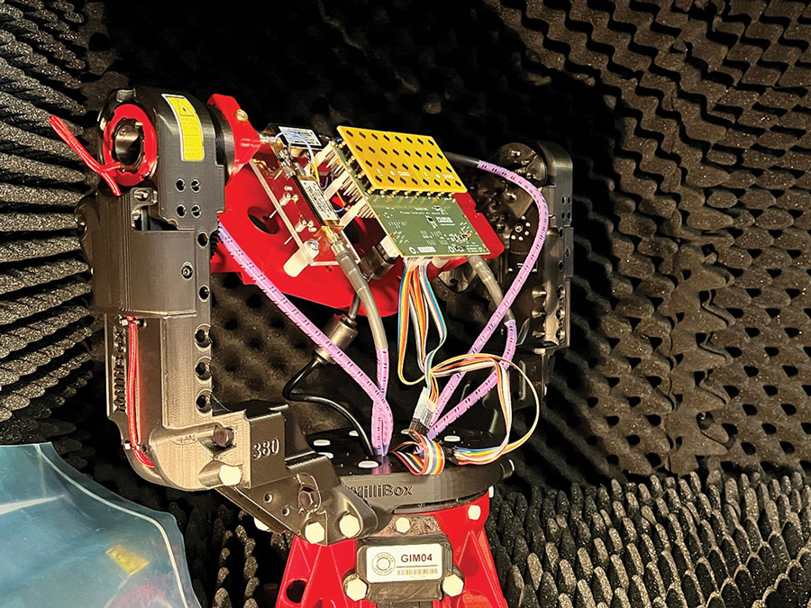
Figure 2c shows the inside view of the anechoic chamber where the gimbal and device under test (DUT) is shown on the left and the fixed horn antenna is shown on the right. The patch antennas of the array are designed with a 45° linear polarization. The transmitting horn antenna is mounted with the same 45° linear polarization to match that of the patch antennas. Additional RF absorbing foam is also mounted on the mechanical fixturing to reduce reflections that would distort measurement data.

Calibration
For all measurements there is a calibration prior to data analysis. The system is comprised of 32 antenna elements, eight BFICs, and one digitizer IC that includes four ADCs and four DACs. Each of the four digitizer IC ADC signal chains include hardened-DSP blocks in the form of DDCs. Within each DDC exist NCOs capable of applying phase shifts on each of the four digitized channels at the subarray level. As such, eight antenna elements form a single subarray as defined for this paper and share a common ADC and DSP signal chain. The phase and amplitude adjustments available in the system are implemented in the analog domain via the BFICs as well as in the digital domain via the NCOs and programmable finite impulse response (PFIR) blocks.
In simplest form, there are three calibration steps:
- Normalize amplitude to the lowest power element via the BFIC variable gain amplifier (VGA)
- Align the digital phase across subarrays via NCO phase shifters (PS) with respect to a natural reference element per subarray
- Align analog phase within each subarray via BFIC phase shifters with respect to a reference element per subarray
Within the analog domain, the BFIC VGA is used to align amplitudes across the entire array and the BFIC phase shifter is used to align phases within a subarray. The NCO shifters in the digital domain are used to align phases across each subarray. The simplified block diagram of Figure 3 highlights the partitioning of the analog and digital domains along with respective signal chain components that enable successful calibration.


Prior to calibration, the array face is positioned such that the received plane wave is at normal incidence. This ensures each antenna element is receiving the same power level simultaneously. The calibration method begins by enabling one analog channel per subarray and postprocessing a complex FFT of the digitized signal for each subarray. For example, Channel 1 of subarrays 1, 2, 3, and 4 is enabled such that a total of four signals are simultaneously digitized by the four ADCs on the digitizer IC. For the next data capture, Channel 1 of each subarray is disabled, and Channel 2 of each subarray is enabled to perform another simultaneous data capture. This method of simultaneous capture is repeated six more times for a total of eight data captures for all 32 elements. The data is postprocessed equalizing the magnitude of all channels to the lowest received power channel using the BFIC VGAs.
Once the amplitude of each channel is equalized, then the simultaneous data capture approach is repeated for phase alignment. Initially, Channel 1 within Subarray 1 is chosen as the natural reference upon which all other channels are phase aligned. The relative phase offset between Channel 1 of subarrays 2, 3, and 4 with respect to Channel 1 of Subarray 1 is calculated and adjusted using the NCO phase shifters in the digital domain to compensate for the relative differences across subarrays.
After the relative phase across subarrays are aligned, then the relative phase within subarrays is determined and compensated using the BFIC phase shifters. This process begins by measuring the phase difference of Channel 2 of subarrays 2 through 4 relative to Channel 1 of Subarray 1. This method is repeated up to Channel 8 within subarrays 2 through 4. Lastly, to align the remaining elements within Subarray 1, the same methodology is repeated utilizing a new calibrated reference such as Channel 1 of Subarray 2. This process concludes a situation where the analog phase adjustments via the BFIC compensate for phase errors within a subarray and the NCO phase offsets via ADC hardened-DSP compensate for phase errors across subarrays.
Once the calibration is complete, the amplitude and phase errors are measured to provide an indicator of the quality. To obtain the amplitude and phase errors, the calibration methodology is repeated with the respective amplitude and phase offsets applied to the hardware. The errors are also used to assess the impact of calibration on the antenna radiation patterns. Table 1 details the amplitude error after calibration. Table 1 and Table 2 are organized to map the error of each channel to the physical position of the antenna elements in the 4 × 8 planar array.
| –0.19 | –0.83 | –0.55 | –0.89 | –0.34 | –0.44 | 0.21 | –0.67 |
| –0.48 | –0.49 | –0.47 | 0.5 | –0.14 | –0.59 | 0.25 | 0.01 |
| –0.5 | –0.69 | –0.5 | –0.58 | –0.16 | 0.2 | –0.42 | –0.2 |
| –0.26 | –0.41 | –0.29 | –0.55 | –0.09 | –0.06 | –0.34 | –0.07 |
Table 1 presents the amplitude error where the amplitude reference channel is located at the linear indexed position 30. The BFIC VGA resolution is less than 0.5 dB per channel and the system amplitude error is nominally biased at –0.20 dB with± 0.70 dB of variation. Table 2 presents the phase error where the natural phase reference channel is located at the linear indexed position 2. The BFIC phase shifters have a nominal phase resolution of 2.8° and the system phase error is nominally biased at –1.79° with ± 2.5° of variation. In both instances, the amplitude and phase error are near the BFIC VGA and phase shifter resolution limits indicating any further reduction of error is limited by the capability of the hardware.
| –1.98 | –0.81 | –0.18 | –3.49 | –1.48 | –2.25 | –3.2 | –3.17 |
| 0 | –2.11 | –1.13 | –1.14 | –0.13 | –1.89 | –3.62 | –1.16 |
| 0.6 | –0.24 | –1.5 | –1.18 | –1.65 | –0.89 | –2.16 | –2.58 |
| –0.06 | –1.24 | –4.29 | –2.13 | –0.09 | 0.72 | –3.72 | –1.17 |
Over-the-Air Beampattern Measurements
Four test cases are measured postcalibration at 10 GHz for two different amplitude taper profiles. Two steering angle positions are measured for each taper profile to provide a direct comparison between the datasets. These test cases are determined to showcase the performance of the array. For an easier comparison between datasets, all amplitude data is normalized to the main lobe peak power of Test Case 1. Table 3 details amplitude taper profile and steering angles for each test case.
| Test Case | Amplitude Taper | Azimuth Steering Angle (°) | Elevation Steering Angle (°) |
| 1 | None | 0 | 0 |
| 2 | Taylor | 0 | 0 |
| 3 | None | 30 | 0 |
| 4 | Taylor | 30 | 0 |
Prior to measurement, a single-patch antenna element pattern and the full hybrid array is simulated at 10 GHz using the MATLAB Phased Array Toolbox. The modeled results provide a baseline to compare measured data against. The simulation is configured for each element with an element factor of cosine0.5 and the phase shifter resolution set to 2.8°. The array model is also partitioned into a hybrid array to match the hardware configuration.
Figures 4 through 7 display the measured 3D beampattern, azimuth slice, and elevation slice for each test case, respectively. In each azimuth and elevation rectangular plot, the modeled element factor, modeled radiation pattern, and measured radiation pattern are overlaid to provide a comparison between modeled vs. measured data. A summary of observations followed with a comparison of key phased array metrics are summarized in Table 4.
Figure 4a displays the measured 3D radiation pattern for Test Case 1. The amplitude weights are set to be equal value across all elements and the receive beam is electronically steered to broadside. Broadside is defined as a steering angle directed to 0° azimuth and 0° elevation. The main lobe peak magnitude is –6.97 dBFS and the first sidelobe level of Figure 4b and Figure 4c is approximately –13 dBc as expected. The modeled and measured data aligns very well for Test Case 1. The null positions match within ±1°. The measured sidelobe levels begin deviating from the modeled predictions at +35° and –55° off axis, but overall maintain a representative radiation pattern for an 8-element array in Figure 4b. The measured elevation data of Figure 4c also aligns very well with the modeled predictions up until approximately ±35° off axis.
The measured 3D radiation pattern for Test Case 2 is displayed in Figure 5a. The amplitude weights for Test Case 2 are weighted for 30 dB Taylor taper and the receive beam is electronically steered to broadside. The typical effects of amplitude weighting are observed in Figure 5b and Figure 5c. The sidelobe reduction of 30 dB is observed at the expected expense of a wider main lobe and lower array gain. Measured data begins deviating from the modeled predictions around approximately ±40° off axis with a noticeable sidelobe peak at –50° of Figure 5b.


Figure 6a presents the measured 3D radiation pattern for Test Case 3 where the amplitude weights are set to equal value and the receive beam is electronically steered to +30° azimuth, 0° elevation. It can be observed that the main beam amplitude is reduced at a rate equal to the element factor and equal to –7.04 dBFS compared to the –6.97 dBFS magnitude when steered to broadside.


Figure 7a shows the measured 3D radiation pattern for Test Case 4. The amplitude weights are set for a Taylor taper with 30 dB side lobe level reduction and the receive beam is electronically steered to +30° azimuth, 0° elevation. Similar effects observed in Figure 5 can be observed in Figure 7. The sidelobe levels are approximately 30 dB below the peak of the main lobe, primarily for the azimuth cut of Figure 7b. Additional widening of the main lobe of the elevation slice and asymmetrical sidelobe levels are noticeable.
| Test Case | Main Lobe Peak Magnitude (dBFS) | Azimuth 3 dB Beam Width (°) | Elevation 3 dB Beam Width (°) | Azimuth First Sidelobe Intensity (dBc) | Elevation First Sidelobe Intensity (dBc) |
| 1 | –6.97 | 13 | 26 | –13.52 | –16.3 |
| 2 | –12.83 | 16 | 33 | –31 | –27 |
| 3 | –7.04 | 13.5 | 30 | –12 | –14.5 |
| 4 | –14.15 | 18 | 40 | 28.2 | –25 |
The deviations of measured data from the modeled data have some possible root causes such as mutual coupling edge effects of a small array and calibration errors. The element pattern of centrally located elements in a very large array tends to have similar element factor responses. The elements located near the edge of an array experience a different environment relative to the central elements due to the asymmetrical environment. The radiation patterns of the edge elements thus differ from the centrally located elements impacting the total antenna pattern. Techniques have been developed to mitigate the mutual coupling effects but were not thoroughly investigated at the time of publication.10,11
For an ideal phased array radiation pattern, it is assumed the elements are all at equal amplitude and an equal phase shift between elements exists. Given the calibration errors measured in Section IV, a Monte Carlo analysis is performed to better understand the impact of the error terms on a theoretical beam pattern. Test Case 3 for both azimuth and elevation slices are simulated with a random amplitude error with a range of ± 0.7 dB and random phase error with a range of ± 2.8°. A total of 100 iterations are analyzed.
The Monte Carlo results for Test Case 3 in Figure 8 and Figure 9 emphasize the influence of amplitude and phase error to the overall radiation pattern. The ideal array model is the black trace, the measured array is the purple trace, and the Monte Carlo iterative results are the remaining traces in both figures. It’s observed in both cases that the amplitude and phase errors negligibly impact the main lobe width and the worst case sidelobe levels are approximately –20 dBc.
The measured azimuth results are proven to be well aligned with the ideal beam pattern when comparing the modeled, measured, and Monte Carlo datasets. Figures 6c and 7c are noteworthy due to the larger deviation between the modeled and measured antenna patterns compared to other data presented. The widening of the main beam of the measured elevation slice is yet to be determined with the data available and any conclusions are speculative at the time of publication.


Beam Squint
Beam squint is prevalent in phased array systems that rely on phase shifters paired with wideband antennas. The time delay required to steer the main beam is a function of linear phase shift vs. frequency, thus, the required timed delay for a beam position can be implemented with a phase shift at a particular frequency for narrow band systems. However, the main beam angular position will be reduced when operating at higher frequencies and increased at lower operational frequencies.7,8,9
The demonstrator hardware used has an approximate antenna bandwidth of 1 GHz centered at 10 GHz. The azimuth radiation pattern of Test Case 3 is measured at 9 GHz, 10 GHz, and 11 GHz to observe the beam squint effect. The predicted impact of beam squint can be calculated directly and is presented in graphic form in Figure 10.


Using Figure 10, the beam angle deviation is approximately +3.75° at 9 GHz and –3° at 11 GHz when the main lobe is steered to +30° for a 10 GHz calibration. The measured angle of the main lobe peak at 9 GHz is at +33° and at +27° for 11 GHz as seen in Figure 11. Noting that the measured angular resolution is 1°, the measured deviations match the expected deviations very well.


To completely mitigate the effects of beam squint, true time delay circuitry for every element is necessary for wideband arrays. Analog phase shifters at the subarray level and true time delay units at the digital level provide a good complexity compromise to mitigate beam squint for hybrid beamforming architectures.
Conclusion
This article details a commercially available 32-element hybrid beamforming demonstrator platform showcasing the receiver over-the-air radiation performance. A unique calibration methodology is leveraged utilizing a synchronous simultaneous data capture to calibrate multiple elements to decrease calibration time. Calibration offsets are enabled via the analog phase shifter and analog variable gain amplifiers at the subarray level. The hardened-DSP of the high speed digitizer also enables digital beamforming capability across subarrays. The modeled and measured results closely align validating the calibration method and the hybrid beamforming capability of the hardware.
About the Authors
Sam Ringwood is a system platforms applications engineer for the Aerospace and Defense Business Unit located in Greensboro, North Carolina. Prior to joining Analog Devices, Sam worked in RF test and RF design roles within ...
Peter Delos is a technical lead in the Aerospace and Defense Group at Analog Devices in Greensboro, North Carolina. He received his B.S.E.E. degree from Virginia Tech in 1990 and M.S.E.E. degree from NJIT in 2004. Peter ha...
Mike Jones is a principal electrical design engineer in Analog Devices working in the Aerospace and Defense Business Unit in Greensboro, North Carolina. He joined ADI in 2016. From 2007 until 2016, he worked at General Ele...
Michael Stetzler is a systems applications engineer in the Aerospace and Defense (ADEF) business and System Platforms Team at Analog Devices in Greensboro, NC. His background is in programming and hardware design and he pr...
Related to this Article
Industry Solutions
Technology Solutions
Product Categories
RF and Microwave
RF Mixers
RF Switches
RF Integrated Transmitters, Receivers, and Transceivers
RF Integrated Transmitters
Direct Digital Synthesis (DDS)
Beamformers, Phase Shifters, and Vector Modulators
Beamformers
Amplifiers
RF Amplifiers
Clock and Timing
Clock Generation and Distribution
D/A Converters (DAC)
High Speed D/A Converters ≥30MSPS
A/D Converters (ADC)
High Speed A/D Converters >10 MSPS
Latest Media 21


