Optimize the MAX2242 PA for 2.4GHz DECT Cordless Phone Applications
Abstract
The main objective of this application note is to provide the overall performance summary of the MAX2242 in non-linear operation. A detailed optimization procedure of the MAX2242 is provided to assist the power amplifier (PA) designer in adapting the PA from Class A biasing (for linear operation) into Class A/B biasing (saturated mode). This note is a useful design tool for PA engineers in applying the MAX2242 to achieve design goals in cordless phone applications with the highest possible performance and lowest possible bill of materials (BOM) cost.
Additional Information:
Introduction
The MAX2242 low-voltage linear power amplifier (PA) was originally designed for the 2.4GHz ISM-band wireless LAN application. With additional PA bias tuning and output matching network optimization, the MAX2242 PA is also ideal for non-linear operation for 2.4GHz DECT (digital European cordless telephone).
The MAX2242 PA consists of a three-stage power amplifier, power detector, power management circuitry, and a shutdown pin. All the above features give the PA designer freedom to meet various system design requirements in cordless phone applications. In addition, the MAX2242 PA features an external bias control pin. Through the use of an external DAC (digital to analog converter), the supply current can be reduced at lower output power levels while insuring the highest possible average efficiency.
Cascading the MAX2242 with the MAX2644 LNA (low noise amplifier) produces a PA that achieves better than 34dB gain and provides 30dB isolation between the transmitter stage and the VCO. This greatly reduces the VCO pulling effect in frequency shift modulation (FSM) systems with time division duplex (TDD) operation that is used in DECT handsets.
The main objective of this application note is to provide the overall performance summary of the MAX2242 in non-linear operation. A detailed optimization procedure of the MAX2242 is provided to assist the PA designer in adapting the PA from Class A biasing (for linear operation) into Class A/B biasing (saturated mode). This note is a useful design tool for PA engineers in applying the MAX2242 to achieve design goals in cordless phone applications with the highest possible performance and lowest possible bill of materials (BOM) cost.
Test Results
At VCC = 3.6V and with RF input power = +4dBm, the MAX2242 is able to deliver +26dBm output power using 290mA supply current (38% efficiency) and 71mA idle current.
The MAX2242 with MAX2644 LNA, at VCC_PA = 3.6V, VCC_Buffer = 2.7V, and PIN = -8dBm, the system delivers +26.15dBm RF output power with 310mA overall supply current and 30dB reverse isolation from the MAX2644.
General Test Condition
All test at room temp.
Test Signals: CW-tone
PA idle current: 71mA
VCC_MAX2242 (PA): 3.6V
VCC_MAX2644 (LNA): 2.7V
POUT: +26.0dBm
Bench Set-up Block Diagram

Figure 1. Set-up diagram.
Test Results
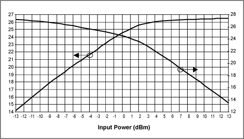
Figure 2. The MAX2242 PA output power and gain vs. input power VCC = 3.6V, frequency = 2450MHz, TA = +25°C.

Figure 3. The MAX2242 PA supply current and efficiency vs. input power VCC = 3.6V, frequency = 2450MHz, TA = +25°C.

Figure 4. The MAX2242 PA output power and gain vs. frequency VCC = 3.6V, PIN = 4dBm.

Figure 5. The MAX2242 PA supply current and efficiency vs. frequency VCC = 3.6V, PIN = 4dBm.
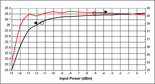
Figure 6. The MAX2242 + MAX2644 cascade POUT and efficiency vs. PIN VCC_PA = 3.6V, VCC_Buffer = 2.7V, frequency = 2450MHz.
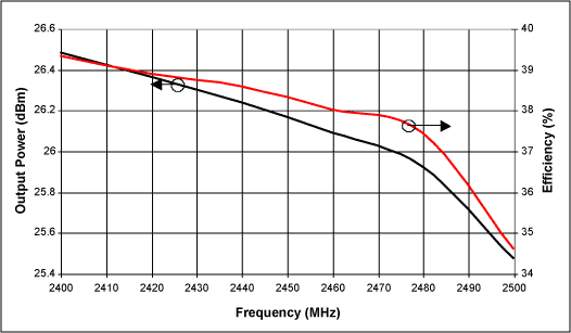
Figure 7. The MAX2242 + MAX2644 Cascade POUT and efficiency vs. frequency VCC_PA = 3.6V, VCC_Buffer = 2.7V, PIN =
Procedure to Optimize The MAX2242 for Non-linear Operation
- Identify the following design specifications:
- Output saturated power level (dBm)
- Input power level (dBm) and required PA gain
- PA efficiency
- Use the MAX2242 standard EV board. Connect the bias control pin to a voltage supply.
- Apply power to the MAX2242 PA.
- Provide the required input power to the PA. In this app note, we use +4dBm as the required input power.
- Adjust the bias control voltage until the desired output power is reached, or maximum available output power with a fixed input power.
- Record the following design parameters:
- VBIAS - Bias Control Voltage
- ICC - Supply current
- IIDLE - Turn-off the input power, and record the Icc
- POUT_SAT - Increase the input power until the output of the MAX2242 reaches deep saturation, and record the RF output power level
- Adjust the output shut capacitor (C2) on the MAX2242 EV board by sliding the location or change the capacitance of the capacitor. By adjusting, the output shut capacitor C2, the PA saturated output power will change as well gain and efficiency. In the MAX2242, there is always a design trade-off in between the maximum saturated output power, gain, and efficiency by adjusting output matching and bias control voltage. It is critical to find out what is the minimum input available power to the MAX2242 to determine the gain requirement.
- Repeat step 5 to step 7 until the desired design specification is met.
- Disconnect VBIAS. Based on the idle current of the optimized performance, change the value of R1 and R2 (same resistance) until the idle current is the same as when the bias control voltage was supplied.
Note: Within the operational frequency range (2.4GHz to 2.5GHz), the MAX2242 is able to deliver a wide range of saturated output power with higher than 38% efficiency. Typical output power range is from +22dBm to +27dBm for optimum operation.
The MAX2242EVKIT Schematic

Figure 8. The MAX2242 schematic.
The MAX2242EVKIT BOM
| Designation | Qty | Description | ||
| * | C2 | 1 | 1.8pF ±0.1pF 50V Ceramic Cap (0402) Murata GRM36C0G1R8B050AD or Taiyo Yuden EVK105CH1R8JW | ECM0033 |
| * | C12 | 1 | 6.0pF ±0.1pF 50V Ceramic Cap (0402) Murata GRM36C0G060B050AD or Taiyo Yuden EVK105CH060JW | ECM0133 |
| * | C3, C6, C8, C10 | 4 | 0.1uF 10% 10V Ceramic Cap (0402) Murata GRM36X5R104K010 or Taiyo Yuden LMK105BJ104MV | ECM0070 |
| C1, C9 | 2 | 33pF 5% 50V Ceramic Cap (0402) Murata GRM36C0G330J050AD or Taiyo Yuden UMK105CH330JW | ECM0066, EC0451 | |
| * | C5 | 1 | 22_F 16V Tant Cap (CASE B) AVX TAJB226M016 | EC0249 |
| C4, C7 | 2 | N/I | ||
| * | L1 | 1 | 10nH ±0.3nH 5% Inductor (0402) Coilcraft 0402CS-10NXJBG | |
| L2 | 1 | 2.2nH Inductor (0402) Murata LQP10A2N2B00 | ||
| R1, R2 | 2 | 8.06KΩ 1% Resistor (0402) | ||
| R3 | 1 | 47KΩ 5% Resistor (0402) | ||
| R4 | 1 | 51Ω 5% Resistor (0402) | ||
| IN, OUT | 2 | SMA Connector (PC Edge Mount) EF Johnson 142-0701-801 DIGI-KEY J502-ND | ||
| JU1 | 1 | 3 pin header Digi-Key S1012-36-ND or Equivalent | ||
| BIAS, PDOUT | 1 | 1 pin header Digi-Key S1012-36-ND or Equivalent | ||
| None | 2 | Shunt for JU1 Digi-Key S9000-ND or Equivalent | ||
| VCC, GND | 1 | Test Points Mouser 151-203 | ||
| * | U1 | 2 | The MAX2242EBC (3x4 CSP) | EU____ |
| None | 1 | The MAX2242 PC Board | ||
| * | None | 1 | The MAX2242 Data Sheet | |
| * | None | 1 | The MAX2242EVKIT Data Sheet | |
| *Supplied by Analog | ||||
Special Assembly Instructions
- C2: Placed at Tick Mark #4
Related to this Article
Products
PRODUCTION
2.4GHz SiGe, High IP3 Low-Noise Amplifier
2.4GHz to 2.5GHz Linear Power Amplifier
Product Categories
Latest Media 21


