Abstract
This application note provides a Bluetooth® history from 1994 to the present, as well as the Ericsson® corporation's role in the system evolution. Bluetooth operates in the ISM band between 2400MHz and 2500MHz, using FHSS on 79 channels with 1MHz spacing. This application note also describes how to use Bluetooth for long-range systems with 100mW output power. An example details a discrete power amplifier (PA), the MAX2240, and the supporting bias and power control circuitry.
This integrated design meets its goals for performance and cost in support of class-1 long-range Bluetooth transmissions.
Introduction
Bluetooth applications in the high-power 100m range require an amplifier capable of 100mW of output power at 2.4GHz. In contrast to traditional design techniques, the MAX2240 power amplifier (PA) for long-range Bluetooth applications features integrated power control, comes in an ultra-small package at low cost, and requires a minimum number of external components.
Background: About Bluetooth
Ericsson Mobile Communications AB (Lund, Sweden) initiated a study in 1994 to investigate the feasibility of a low-power, low-cost radio interface between mobile phones and their accessories.1 The intent of the radio interface was to eliminate cables between mobile telephones and personal-computer (PC) cards and headsets. Initially, the link was called the multicommunicator (MC) link. As work on the new wireless link progressed, it became clear that there was no limit to the kinds of applications that could use a short-range radio link. An inexpensive short-range radio technology would make communications between portable devices economically feasible. However, for the system to succeed, a critical mass of industry support was necessary. In 1997 Ericsson approached other manufacturers of portable devices to raise interest in the technology, and in 1998 a special interest group (SIG) comprised of companies from the mobile telephone and computer industry (Ericsson, Nokia®, Intel®, Toshiba®, and IBM®) was created. The consortium was formed to establish a de facto standard for the air interface and the system software, and to promote the technology. In May 1998 the SIG publicly introduced the new wireless connectivity solution. The SIG called the short-range wireless connectivity solution "Bluetooth" after the tenth-century king who united Denmark.
The Bluetooth system operates more or less in the unlicensed industrial-scientific-medical (ISM) band from 2400MHz to 2500MHz, with slight variations throughout the world. The system incorporates a frequency-hopping spread-spectrum (FHSS) scheme to share the spectrum among multiple users and to legally occupy the band if the radio-transmit power exceeds 0dBm (1mW). A total of 79 hop channels are used, with channel spacing of 1MHz and two-level frequency-shift-keying (FSK) modulation. The system achieves a bit rate of 1Mbps and employs Gaussian modulation filtering with a bandwidth-time (BT) product (bandwidth per bits) of 0.5.
The system employs an air interface similar to that used in existing IEEE® 802.11 FHSS wireless local-area-network (WLAN) systems; some changes enable use of low-cost hardware (for example, relaxed sensitivity, relaxed image rejection, and frequency hopping every packet with no fast turnaround time). However, the channel frequencies are the same and the modulation scheme is essentially the same as for two-level FSK. These modulation characteristics establish the type of amplifier required on the transmitter. A constant-envelope FSK modulation scheme is employed in Bluetooth, permitting the use of a saturated-mode transmit amplifier.
Bluetooth for Long-Range Applications
The Bluetooth system was originally conceived as a short-range link (up to 10m). However, as the possible Bluetooth applications expanded, potential end users expressed the desire for greater range. Given that the system’s receiver sensitivity is fixed at -70dBm, the practical solution to increasing range was to increase the radio transmit power. The need for greater transmit power led to the definition of an additional class of radio-transmit output power. A peak transmit power of 100mW versus 1mW was chosen to ideally provide approximately a 10x improvement in range to 100m, and to keep the transmit power within the European ETSI regulation of 100mW effective isotropic radiant power (EIRP). The higher output created the need to add a separate PA after the RF transceiver (Figure 1). The higher transmit-power level became part of the Bluetooth radio-interface specification, and is defined as class-1 operation.

Figure 1. Bluetooth radio system diagram.
The class-1 transmit-power specification is detailed in the radio section of the 1.0 version of the Bluetooth specification.2 The output power is limited to a maximum transmit output power of 100mW. If class-1 power is used, the specification requires the transmitter to implement power control to minimize overall interference and optimize the radio power consumption. The Bluetooth transmit specifications establish requirements for the overall radio. The PA specifications are derived from the system requirements and component characteristic of the elements that follow the PA (Figure 1). The RF switch, the RF bandpass filter, and the connector contribute a power loss of approximately 3dB (Figure 2).

Figure 2. The Bluetooth front-end can be simplified to this representation.
Various specifications impact the transmit PA, including those covering spurious emissions and other operating conditions. All amplifier output specifications imply the use of modulated signals. In addition to the Bluetooth radio specifications, some specific system requirements arise from the implementation of a Bluetooth radio. The PA operating conditions include a supply voltage of +2.7VDC to +5VDC; a temperature range of -20°C to +60°C; input-power levels of 0dBm to +4dBm; supply current of less than 140mA; and target efficiency of 30% to 40%. The PA must provide an on-off control to permit power-down during the receive timeslot. The PA should turn on/off in several microseconds. In the power-down mode, the PA collector current (ICC) should be less than 10µA. PA implementation objectives include a cost of less than $1.00 (U.S.), a size of less than 10mm x 10mm, and a solution-design time of no more than one week.
Radio-transmit output-power specifications are implied over all operating conditions of supply voltage, temperature, and frequency. All power is measured in a 100kHz bandwidth. The minimum transmit output power is 0dBm, whereas the maximum transmit output power is +20dBm. The power can be controlled monotonically from +4dBm to +20dBm in minimum steps of 2dB and maximum steps of 8dB.
In-band spurious levels refer to the permissible levels of adjacent- and alternate-channel power, as well as any residual spurious signals within the 2400MHz to 2500MHz band. The primary regulatory limit is the -20dBc spectral power limit at the 1MHz band edge. All specifications are measured with an input signal that adheres to the Bluetooth modulating signal characteristics. All out-of-band spurious emissions refer to signals that are outside the 2400MHz to 2500MHz band. These specifications include maximum spurious levels of -36dBc from 30MHz to 1GHz; a maximum of -30dBc from 1GHz to 12.75GHz; and at least -47dBc from 1.8GHz to 1.9GHz, and from 5.15GHz to 5.3GHz.
Classical Approach
The "classical" or traditional approach to designing a PA with power control centers around a two-stage PA constructed from discrete power transistors and passive elements or, more recently, with PA integrated circuits (ICs) packaged in modest-sized plastic packages (for example, 8-pin SO or MLP16 packages). This PA approach provides only the RF signal path, basic biasing, and rather rudimentary analog power control. Implementation of the Bluetooth 100mW class-1 specification for power control requires additional circuitry to implement the full power-controlled transmit-amplifier function.
Given an open-loop PA with an analog power-control input, the power detection, power-level setting, and closed-loop control scheme are implemented with external circuitry. A simple square-law diode detector is often used to detect power over a limited range and to produce a voltage output proportional to the PA output power. Commonly, the detector voltage is compared against a set voltage level that corresponds to a desired PA output-power level. An op amp, configured as an integrator, serves as a closed-loop control amplifier to drive the analog control input until the detected voltage equals the set voltage. A possible implementation of such an approach includes a 2-bit digital control (Figure 3) using a temperature-compensated diode detector.3

Figure 3. Classical power-control PA solution.
It is evident that the traditional approach requires a significant number of external components to fully implement the power-control function and digital interface: detector diodes, capacitors, resistors, an op amp, and a digital-to-analog converter (DAC). Although the configuration can be designed to work acceptably, the classical power-control solution has several disadvantages that make it unattractive for Bluetooth systems. The primary disadvantage is that the bill-of-materials (BOM) cost is far too high. An approximate high-volume BOM cost for the circuit in Figure 3 is $1.76, including the PA. Bluetooth SIG members have stated a target cost for the Bluetooth radio at $5.00,4 and the PA cannot possibly account for one-third of the total cost.
Another disadvantage of this solution is that the required printed-circuit-board (PCB) area is relatively large. Most Bluetooth radio implementations must fit into a small space, such as a module. Here, the total RF module footprint is perhaps as small as 10mm x 14mm.5 The circuit in Figure 3 will likely consume that area itself. The combination of the large plastic package for the PA, the external matching, and the discrete power detection and control circuitry limit the minimum footprint area.
Additionally, the discrete approach shown is very design-intensive. A significant amount of time must be devoted to working with the practical circuit to achieve accurate power detection, stable closed-loop control, and establishment of the desired digitally-controlled power levels. Numerous adjustments to the circuit component values and PCB implementation will certainly be needed before a specification-compliant class-1 power-control solution is reached. These disadvantages are not acceptable for Bluetooth radio projects and/or Bluetooth-enabled products. Bluetooth radios must be inexpensive, small, and developed in a timely fashion. Realistically, the radio designer requires an alternative solution for the Bluetooth class-1 PA function.
New Solution
A novel PA IC developed at Maxim specifically addresses the Bluetooth system requirements and the specific needs of the Bluetooth market. The MAX2240 PA IC eliminates the major disadvantages associated with the classical approach; it introduces a new form factor and cost structure for a PA solution. The MAX2240 single-supply PA is designed specifically for Bluetooth systems, although it can be used for other FSK modulation systems operating in a 2.4GHz to 2.5GHz ISM band. The PA provides nominal +20dBm (100mW) output power in the highest power mode at VCC at +3VDC.
The MAX2240 uses a new architecture in which the power-control function is combined with the PA on the same IC (Figure 4). The architecture fundamentally streamlines the overall PA solution. The core PA stages are combined with an open-loop digital power-control scheme and a shutdown/bias control. Two digital control bits (D0, D1) control four distinct output-power-level states. The digital power-control inputs are decoded to drive a variable-gain-amplifier (VGA) stage in the RF path and, consequently, the output power. The four states provide a well-defined output-power level versus a digital code setting with power steps approximating 6dB/step. The output-power levels are first-order optimized over input power, temperature, supply-voltage range, and manufacturing variations.

Figure 4. This simplified block diagram represents the MAX2240 low-cost Bluetooth PA.
In addition, the application is greatly simplified with the inclusion of temperature- and supply-independent biasing, and integration of the RF input and the interstage matching. An on-chip temperature- and supply-stable bias circuit maintains stable and predictable PA performance for all operating conditions; it eliminates externally applied bias voltages or currents. The IC operates from a supply of +2.7VDC to +5VDC, enabling it to run directly off an unregulated battery voltage in the host mobile-communication device. Most of the RF signal-path impedance-matching circuitry is integrated. The output stage match is not integrated in the chip, in order to achieve the best PA efficiency and permit trade-off in output power, harmonics, and efficiency.
The PA offers a digital shutdown (enable) control input so that it can enter either active or shutdown mode, selected by the baseband IC. In shutdown mode, the supply current is reduced to approximately 0.5µA. This digital shutdown control permits the PA to be turned on during the transmit timeslot and off at all other times, thereby minimizing the overall radio-current consumption.
Undoubtedly, the most advanced aspect of the MAX2240 PA is the use of chip-scale packaging (CSP). This package is an IC die-level packaging technology where solder bumps are attached to the bond pads of the IC through a special post-processing step while the chips are still in raw wafer form. The bumps are placed at a standard lead pitch of 0.5mm in a grid array. The MAX2240’s grid is a 3 x 3 array of nine solder bumps with an ultra-small 1.56mm x 1.56mm net chip/die size (UCSP™ package). After the solder balls have been attached, the wafer is cut up, converting the IC to die form. In die form, the chip is ready for direct mounting to the printed-circuit board (PCB), similar to a conventional surface-mount device. The device is placed on a pad layout and is IR solder reflowed with the other components on the PCB, directly mounting the chip to the PCB. The chip-scale devices are shipped in tape and reel, similar to other surface-mount devices. An index-area marking is placed on the backside of the die to denote the A1 pin of the die. The use of CSP technology creates the industry's smallest PA IC product, helping speed Bluetooth class-1 integration into mobile telephones, laptop computers, personal digital assistants (PDAs), and other portable devices.
The MAX2240 is designed for straightforward application integration and design-in (Figure 5). The device operates from a single, positive supply voltage (VCC). Each supply-voltage connection requires an RF bypass capacitor (typically 220pF) to ground. On the VCC pin, a small 1.2nH series inductor (board trace) and shunt 18pF capacitor are recommended to optimize PA performance. The RF input (RFIN) features an internal impedance-matching network and a DC-blocking capacitor. Therefore, it is possible to directly connect a 50Ω transmission line to RFIN.
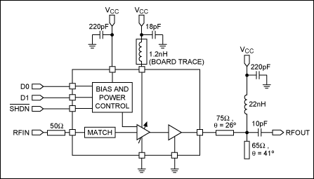
Figure 5. MAX2240 application circuit.
The output stage of the MAX2240 is the collector of the output transistor. The DC bias and impedance matching are applied externally to the chip to achieve higher efficiency and output power than is possible with integrated, low-matching elements. Optimum performance occurs at an impedance presented to the PA’s output transistor. At 2.45GHz, this impedance is 15.2Ω + j17.9Ω looking into the matching network loaded with 50Ω. The primary power-matching structure is a lowpass network, formed by the series transmission-line section T1 and the open-stub transmission-line section T2. The transmission-line network acts similar to a series inductance and shunt capacitance.
Transmission lines T1 and T2 are expressed as electrical lengths of a particular characteristic impedance line, but could be designed with different impedance lines. The length of T2 should be chosen to provide a short circuit at the second-harmonic frequency of the fundamental and to significantly attenuate its amplitude at the output: a quarter-wavelength at the second-harmonic frequency of 4.9GHz. The third-harmonic frequency is attenuated through the parasitic capacitance in the choke inductor. This capacitance rolls off the choke impedance at higher frequencies and appears as a low impedance at the third-harmonic frequency. The output series capacitor is used as a DC-blocking capacitor and a final matching element. Here, a value of 10pF is recommended. The output stage also requires a connection to VCC through an inductor (recommended as 22nH). The exact value is not critical, but should provide an impedance of several hundred Ω at 2.4GHz and be self-resonant at or below 2.4GHz. Finally, all digital inputs are compatible with complementary-metal-oxide-semiconductor (CMOS) logic levels and designed for direct connection to the digital baseband IC.
The advantages of the new PA approach are evident when comparing it to the classical closed-loop PA solution. An examination of the BOM cost, PCB size, and design time clearly shows that there is a dramatic overall improvement for the new approach compared to the classical PA solution (see Table 1 below).
| MAX2240 | Classical PA Solution | ||||
| No. | Component | Cost ($) | No. | Component | Cost ($) |
| 1 | Power amp IC | 0.75 | 1 | Power amp IC | 0.75 |
| 4 | Power amp IC solution | 0.04 | 1 | Om amp (low VOS) | 0.3 |
| 1 | Capacitors | 0.05 | 2 | Detector diodes | 0.13 |
| Inductors | 2 | PNP transistors | 0.1 | ||
| 2 | Inductor | 0.1 | |||
| 9 | Capacitors | 0.09 | |||
| 8 | Resistors | 0.04 | |||
| Total BOM cost | 0.84 | Total BOM cost | 1.76 | ||
The MAX2240 reduces the BOM cost for the Bluetooth PA implementation by eliminating the need for detector diodes, op amps, resistors, capacitors, and DAC components. Only a few bypass capacitors and a simple output-matching network are required to appropriately apply the MAX2240. This simplification results in a BOM cost that is half the cost of the classical approach. A BOM cost of less than $1.00 supports efforts to achieve the Bluetooth radio-cost goal of approximately $5, and establishes a path for further cost improvements.
A first-order estimate of the PCB area required for application of the classical PA solution and the MAX2240 shows a large difference in the solution footprint. The classical PA approach requires a PCB space of approximately 10mm x 14mm (140mm²) to implement the example shown in Figure 3. In contrast, the MAX2240 requires a footprint of approximately 4mm x 8mm (32mm²), only a quarter the area of the classical approach. This small size makes the MAX2240 ideal for integration into modules.
Related to this Article
Products
Product Categories
{{modalTitle}}
{{modalDescription}}
{{dropdownTitle}}
- {{defaultSelectedText}} {{#each projectNames}}
- {{name}} {{/each}} {{#if newProjectText}}
-
 {{newProjectText}}
{{/if}}
{{newProjectText}}
{{/if}}
{{newProjectTitle}}
{{projectNameErrorText}}
Latest Media 20


