Noise from Different Switching Regulator Topologies
Many different switching regulator topologies exist. Some, such as the classic stepdown converter, also known as a buck converter, are very widespread. However, there are also a few lesser known switch-mode dc-to-dc converters, including the zeta topology. Differentiation can be made between basic and extended topologies. The basic topologies use just two switches, one inductor, and two capacitors. These are nonisolated switching regulators; that is, switching regulators that are not galvanically separated. The buck converter, the boost converter, and the inverting buck–boost topology are included in this category. All other topologies require additional components. A SEPIC converter, for example, also needs a coupling capacitor and a second inductor. Besides the nonisolated switching regulators, there are those in which a transformer is used to realize galvanic isolation.
For circuit designers, a power supply is often considered a black box, or a 4-pole element. It has two input lines and two output lines. Figure 1 shows a symbol for a block diagram of a dc-to-dc converter. A dc-to-dc converter that is not galvanically isolated is shown at the top, and a galvanically isolated converter is shown at the bottom of the figure.

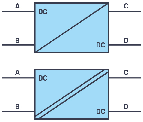
Figure 1. A switch-mode power supply shown as a black box.
In Figure 1, noise information is not conveyed, with respect to the terminals. Different switching regulator topologies have different behavior in terms of the terminals of the 2-port network. Figure 2 shows a universal step-down converter, the ADP2441 from Analog Devices, for industrial applications. It converts 24 V at the input to 3.3 V at the output. With this topology, it can be seen that the input side generates pulsed currents and thus is very noisy. When the high-side switch on the ADP2441 is on, current flows into terminal A. When this switch is off, no current flows through node A. On the output side C, however, there is very little noise. Here, an inductor in the output path ensures that there is no pulsed current on the output side.

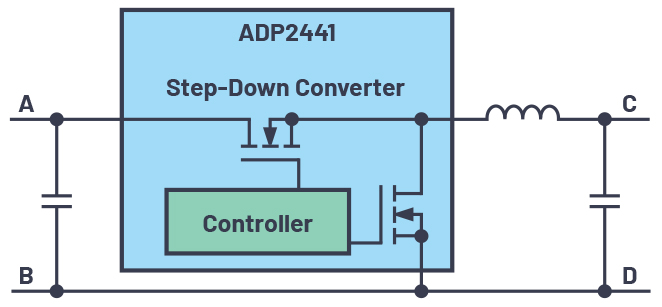
Figure 2. Practical design of a switching regulator topology.
Table 1 was compiled so that system designers can get valuable information on the basic behavior of switching regulators in the conceptual design phase. The most common switching regulator topologies are listed here. The first row indicates whether or not the noise level is low on the input side, that is, at terminals A and B of the 2-port network. The second row indicates whether the respective topology has high or low noise on the output side, that is, terminals C and D of the 2-port network. Table 1 shows the low and high noise levels.
| Buck | Boost | Inverting Buck–Boost | Flyback | SEPIC | Cuk | Z4-Switch Buck–Boost | |
| Input-Side Noise | High | Low | High | High | Low | Low | High |
| Output-Side Noise | Low | High | High | High | High | Low | High |
Through additional filtering, for example, with separate LC filters, conducted noise can be greatly reduced in a switching regulator circuit. In this way, the weaknesses indicated in Table 1 can be counteracted. Nevertheless, system designers should recognize which dc-to-dc converters have especially high noise levels at which terminals. By knowing this, they can plan in advance for the corresponding filter and the necessary additional space these filters occupy.
About The Authors
Related to this Article
Product Categories
{{modalTitle}}
{{modalDescription}}
{{dropdownTitle}}
- {{defaultSelectedText}} {{#each projectNames}}
- {{name}} {{/each}} {{#if newProjectText}}
-
 {{newProjectText}}
{{/if}}
{{newProjectText}}
{{/if}}
{{newProjectTitle}}
{{projectNameErrorText}}
Latest Media 21


