Abstract
With the introduction of the new AISG v3.0 standard in 2019, many new use cases were implemented for antenna line communication. While these changes had little to no impact on the physical layer of operation, one systematic change was obvious: every RF connection on the cellular tower would now require AISG communication to service the PING function. This application note summarizes some of the changes on the hardware level and shows how features of the new MAX11947, an AISG modem with a 4:1 multiplexer, can help system designers implement the new standards requirements with fewer components and less development overhead.
Introduction
The proliferation of cellular networks and handsets throughout the world, especially over the past decade, has resulted in an exponential need for electronics to support the mobile communications infrastructure. A simultaneous demand for more bandwidth is also pushing network providers to continuously expand their coverage while increasing cell density, which in turn, has boosted the need for infrastructure hardware.
Over 15 years ago, manufacturers began to standardize interoperability of cellular radio equipment, allowing more variation in assembling cellular base stations with antenna gear, amplifiers, etc. This communication standard was first established by the Antenna Interface Standards Group (AISG) back in 2003 and 2004[1]. The AISG standard continues to evolve with market expansion and this application note introduces several features of the MAX11947 modem used to meet the interoperable communications needs of today and into the future.
AISG v2.0 and the Physical Layer Modem
Integrated modulator-demodulators (modems) were introduced in 2009 to provide a complete, focused solution for translating between the ubiquitous RS-485 interface and a 2.176MHz OOK signal which piggybacks on the cellular band RF cable within a single circuit. The IC solution allowed for a much more compact system design, saving space, power, and hardware while the integrated modem provided the reliability of a simple, proven, factory-tested device.
The New AISG v3.0 Standard
An upgrade to the successful standard was put forth by the AISG in 2019. This evolutionary step built upon the success of previous generations with the intent to add new features while maintaining the core interoperability of primaries and their managed antenna line devices (ALDs).
The new AISG v3.0 feature set includes device discovery, connection mapping, and multi-primary control. While a system designer will find the new standard to be a helpful upgrade for many higher-level functions, the PHY layer remained unchanged from v2.0 to v3.0[2][3]. Consequently, the original modems are still fully compatible with the new AISG v3.0 standard.
The Need for More than One AISG Channel
The jump from AISG v2.0 to v3.0 had very little impact on the physical layer of the system. However, included in the new standard is the requirement for each channel to be AISG-aware so the overall system can map connections with ping packets. This helps with the build-out of the overall radio system but places an additional burden on the hardware designer to include the AISG communications on all the RF channels where previously it was only necessary on one.
Trying to convert an AISG v2.0 system design directly into a v3.0-compatible application could require twice as many, or more, modems as a previous generation design; going from six modems (grey blocks) up to 15 in the example shown in Figure 1 (grey plus red blocks).
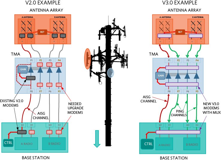
Example application of AISG v2.0 vs. v3.0
In this example, two modems would still be needed per antenna pair to maintain compatibility. However, now up to seven or eight modems would be required on the Tower Mounted Amplifier (TMA) with four listening on the ports running to the antenna array (upstream) and four used on the downstream ports, which are for broadcasting a ping to the base station. The base station would also require additional modems, one for the original AISG channel, and three more to receive ping packets from the TMA on the other ports.
Obviously 15 or 16 modem ICs would be excessive since that total count could be reduced by using bypass circuits and/or RF switches to share AISG signals between RF ports.
Adjustable Transmitter Power
Even with the older AISG designs, there was an inherent need to adjust the output level of the transmitter's power amplifier (PA). This was commonly required whenever a splitter was used for circuits such as the bypass channel shown in the v2.0 TMA example of Figure 1. Signal power adjustment would also be helpful if there were excessive attenuation at the 2.176MHz channel from RF filtering or lossy connections. The original modems provided such adjustability through external resistors used to set the PA bias point, allowing the modem to meet the AISG signal requirements (see Figure 2-A and 2-B).

Transmit power and receive threshold
Spectral Emissions
A primary requirement of the AISG standard for the PHY layer is the spectral purity of any modem's transmitter. The spectral performance is addressed in the AISG v3.0.0.3 standard within Section 10.3.11 - Modular Characteristics. These strict requirements limit the PA's out-of-band spectral emissions and tend to be very stringent, especially at the 30MHz knee where any harmonic noise must be below -67dBm in power and where the resolution bandwidth (RBW) settings of the test instrumentation are the most stringent. The PA output spectrum also must be balanced with the overall power level given the absolute limits in the spectral mask.

Figure 3. AISG v3.0 standard modem spectrum emissions mask.
Power Savings
Power savings is always high on a system designer's list of requirements. Often there is a power budget constraint which applies pressure on more critical design elements, especially as the ALD hardware is scaled to more channels at the same time they are becoming ever more compact. Having some flexibility in less critical circuits can give the designer more freedom on important blocks in the power budget.
One of the original AISG v2.0 modems on the market had a lower-power standby mode, while another had no ability to control the power other than fully shutting down the device.
Sharing the Reference
Every AISG modem requires a reference signal to generate the 2.176MHz carrier. This is typically provided with an 8.704MHz crystal and an integrated oscillator circuit. All ICs on the market can be architected with a primary/secondary (or master/slave) circuit within the AISG system, saving crystals, and thus reducing BOM costs.
Each chip can act as the primary crystal oscillator (XO) for downstream modems by buffering the signal through their SYNCOUT pin. This SYNCOUT signal is an open-drain output which requires a simple external pullup resistor to the analog supply so it can operate properly. This signal is then propagated to additional secondary modems in the system.
Upgraded Features Available in the MAX11947 AISG Modem
Maxim Integrated introduced the first AISG v2.0 modem with the original MAX9947. This device still provides a complete solution for interfacing between RS-485 and the defined 2.176MHz OOK signal and thus, remains fully compatible with the new AISG v3.0 standard.
So why the new design?
Even though Maxim's original modem can service the new standard, the expanded feature set in v3.0 provided an opportunity to improve the modem as well. Because of this, Maxim designed the new MAX11947 with several performance improvements and added features. As a first step, a digital interface was added to the modem along with several internal configuration registers. This new SPI control allowed for the integration of features which were previously managed with external parts such as the PA power bias network. This is now incorporated as a digitally adjustable transmit power and includes another feature to match the adjustable PA power, an adjustable receive sensitivity threshold. We included the PA output resistor to remove one more external component from the designer's bill of materials (BOM) and most importantly, the biggest feature added to the device was an integrated 4:1 port multiplexer. The new MUX effectively provides four modems in one chip and facilitates an automatic scanning capability giving the developer a tool to interact with up to four RF ports to meet the new ping requirements of AISG v3.0.
Integrated 4:1 Multiplexing
The v3.0 requirement to initiate and detect a ping packet on all the connected RF channels will allow the end user to map cable connections, identify multiple primaries and secondaries, and find faults in the interfaces during initial assembly, etc. As mentioned earlier, adding 16 modem ICs in the example would be excessive and could be more easily met using RF switches to share a AISG modem between ports. This became the primary motivation for a new, more integrated device.
That is where the new MAX11947 comes in. The integrated 4:1 MUX provides built-in switching capability, greatly reducing the need to specify and test additional circuits while lowering, rather than increasing, the BOM requirements. In the earlier example, what was six modems in the AISG v2.0 system and potentially 16 modems required for a v3.0-capable system has been reduced to just five MAX11947 modems total because of its multiplexing capability (purple blocks in Figure 1).
Automatic Port Scanning
Integrating a 4:1 MUX with our high-performance AISG modem allowed Maxim to also include a purpose-built finite state machine to drive all the components in unison. The new MAX11947 provides a code-free, non-microcontroller-based means to scan ports and identify a ping carrier signal with very little user intervention. The automatic port scanning feature will help to both map the hardware interconnects and find faults with the RF cabling system—completing the process with fewer IC components than would otherwise be required.
For more details on the port scanning features, refer to the "Port Scanning" section of the MAX11947 data sheet and see Application Note 7428: Port Scan Operation of the MAX11947 for specific details.
Internally Adjustable TX Power
The MAX11947 has the same adjustability to the transmitter output power as the original MAX9947 modem but now the adjustment is made through the SPI interface rather than requiring fixed resistor values to be included with the system design. By changing a programmable value in a register, the output can be adjusted from about -0.5dBm to about +7.0dBm in 0.5dB steps (the highest power depends upon the supply voltage). This digital control of the TX power gives the system designer on-the-fly power adjustment capability, which in theory, would permit better performance once installed in the field. This adjustable power also allows the designer to accommodate a signal splitter for a bypass channel while still meeting the AISG transmitter power requirement (see Figure 2B).
For more details on this adjustable TX power, see the "Output Power Control" section of the MAX11947 data sheet.
Added Adjustability to the RX Threshold
Like the transmitter adjustable output power, the receiver threshold could be affected by power splitters, inline filtering, or other attenuation factors on the RF channel. Unfortunately, there was no adjustability of the ON/OFF threshold in the original MAX9947 modem.
Another feature of the MAX11947 is the ability to independently adjust the RX comparison level just like the TX power. This is also accomplished by programming an internal register, allowing the carrier detection threshold to range from -15dBm down to -21.5dBm. The modem also permits RX adjustments on-the-fly, again permitting the system designer to pass this flexibility on to the end user.
For more details on the adjustable RX sensitivity threshold, see the "Input Range and Sensitivity Threshold Control" and "In-Line Attenuation" sections of the MAX11947 data sheet.
New Power-Saving Modes
The original MAX9947 provided only one mode of operation, either it was powered up and ready to receive and transmit, or it was shut down with no functionality. The MAX11947 incorporates several power modes: operational, standby, and power-down. This gives the system designer many choices to save power.
The full operational mode works as the name implies—everything in the device is running, including the transmitter and receiver paths, the crystal oscillator, and SYNCOUT system (primary/secondary used by one crystal oscillator), plus the digital registers and serial interface.
In contrast, the standby mode disables the transmitter circuitry. Since the modem will spend most of its time listening for an incoming message on the RF port, using the standby mode can save significant power, typically a 11mA lower current draw versus the full operation mode. This lets the system continually listen for an OOK signal at a lower power setting and once an outgoing message is imminent, the transmitter circuit can be enabled.
Even more power savings is realized by disabling both the transmitter and the receiver circuitry using the power-down mode. This mode can maximize the power savings (typically 20mA lower than operation mode) while still allowing the modem to act as a primary oscillator for others downstream. If the SYNCOUT buffer is also shut down, the system designer can save more than 23mA versus operational mode.
For more details on the various power-saving modes, refer to the "Standby and Power-Down Operational Modes" section of the MAX11947 data sheet.
Improved Spectral Performance
The MAX9947 met these mask requirements while providing a narrow 1~2dB of margin at the 30MHz inflection point. Similarly, a competitive AISG modem provided around 4dB of margin.

Figure 4. Comparative spectral performance.
The MAX11947 exceeds the compliance of the previous generation modems, giving the system designer about 15dB of margin to the spectral mask at the 30MHz point.
Buffered SYNCOUT and Continued Operation
Both the MAX9947 and MAX11947 can be used in a primary/secondary configuration, saving crystals, and thus reducing BOM costs. The original MAX9947 was hampered by not having a low-power mode that could allow the XO circuit to operate yet save power.
With the MAX11947, this deficiency has been solved. The new modem offers both a standby and power-down option which include the ability to use the oscillator circuits when these low-power modes are engaged.
Another feature available in the new MAX11947 is an adjustable SYNCOUT drive capability. By modifying a register value, the user can either disable the output (saving even more power), leave it set to the default drive level (which matches the original MAX9947), or it can be boosted to either 2x or even 4x the normal drive current. To maintain the same output voltage levels for the open-drain signal, the pullup resistor must be adjusted proportionally. For example, with the normal 1x setting, the recommended pullup resistor is 1k? while in the 4x current mode, the pullup resistor should be reduced by a factor of 4, thus a 250? resistor. This total pullup value can be implemented as four parallel 1k? resistors distributed in a "star daisy-chain" topology as shown in Figure 5. This may be helpful if there are long trace distances between the primary and secondary modems.

Figure 5. Distributed SYNCOUT star daisy-chain.
For details on the oscillator circuit shutdown, see the "Power-Down Mode" section and for the buffered SYNCOUT operation, see the "Clock Master/Slave Configuration" section of the MAX11947 data sheet.
Alternate Modem Interface
Controlling the original MAX9947 was a simple process: connecting an RS-485 driver or a microcontroller (MCU) to the classic RS-485 interface signals via the TXIN, DIR, and RXOUT pins. The same process can be duplicated with the new MAX11947 although now those same signals are also mirrored within the SPI registers. This means that additional GPIO, UART, or other port pins are not required to interface with both the SPI and classic modem signals.
By reading from the mirrored DIR and RXOUT bits and writing to a TX_ON bit, both interface and control can be exercised through the registers. The system designer now has the option to use the modem as a bridge between an RF port and an MCU with minimal resources.
For more details on using the modem without interfacing to the traditional RS-485 modem pins, refer to the "Alternate Modem Interface" section of the MAX11947 data sheet.
Conclusion
The MAX11947 has been purpose-built to meet the needs of the new AISG v3.0 system designer. It provides added benefits that expand the roll of the modem and offers new built-in flexibilities which go beyond just saving design time and BOM cost.
Related to this Article
Product Categories
{{modalTitle}}
{{modalDescription}}
{{dropdownTitle}}
- {{defaultSelectedText}} {{#each projectNames}}
- {{name}} {{/each}} {{#if newProjectText}}
-
 {{newProjectText}}
{{/if}}
{{newProjectText}}
{{/if}}
{{newProjectTitle}}
{{projectNameErrorText}}
Latest Media 21


