Abstract
Offering higher bandwidth than its voltage-feedback counterpart, the second-generation current conveyor operational amplifier (CCII) can be used in RF mixers, high-frequency precision rectifiers, and medical applications such as electrical impedance tomography. The conventional operational amplifiers cannot be used in the high-frequency applications due to their limited gain-bandwidth product.
Introduction
The current conveyor has been around since the original design, or CCI (which can be regarded as an ideal transistor), was initially proposed by Smith and Sedra in 1968¹,². CCI was then replaced by a more versatile second-generation device in 1970, the CCII³. Current conveyor designs have mainly been BJT due to their high transconductance values compared to their CMOS counterparts. They are used as current-feedback operational amplifiers such as the MAX4223 low-power amplifier, which features current feedback rather than the conventional voltage feedback used by standard operational amplifiers. This means that the current feedback operational amplifier is not restricted by the conventional gain bandwidths of a standard operational amplifier, and can offer a much higher bandwidth solution than its voltage-feedback counterpart.
Current conveyors are used in high-frequency applications where the conventional operational amplifiers cannot be used, because the conventional designs are limited by their gain-bandwidth product. In theory, the current conveyor is only limited by the ft of the transistors used in its design. Some applications where current conveyors are used today include RF mixers, high-frequency precision rectifiers, and medical applications such as Electrical Impedance Tomography (EIT).
A Bipolar Conveyor
The diagram in Figure 1 below shows a current conveyor implemented using bipolar devices.

Figure 1. A bipolar CCII.
From Figure 1 it can be seen that the CCII conveyor can be modelled as an ideal transistor:
Y being the base/gate
X being the emitter/source
Z being the collector/drain
This type of circuit works well as a circuit with BJTs, as the transconductance and Early voltages of BJTs are much greater than that of CMOS devices. Therefore, current conveyors work well as source followers. Gain X/Y is close to 1; Z has a natural high-output impedance which cannot be mimicked by their CMOS counterparts.
The CMOS Source Follower
As previously explained, the major problem with a CMOS follower is the low gm and poor Early voltage (1/lambda). This equates to poor gain, because the gain for a voltage follower heavily relies on these two parameters to be large. This can be observed in the equation below:

Where gL is the load conductance, gds is the drain source conductance and gm is the transconductance of the CMOS device.
A typical simulated gain with a TSMC 0.18µm with a load of 1kΩ gave a gain of 0.7. Compared to the ideal gain of 1, this represents a 30% loss in output gain.
Current Conveyor Source Follower
One can use an unbuffered amplifier (Figure 2a) to mimic a source follower with a gain of one. Then this modification can be added to the basic design in Figure 1 to make a CCII current conveyor.

Figure 2a. A simple source follower.
Figure 2a can be implemented as shown below in Figure 2b.

Figure 2b. The CCII unbuffered source follower and implementation.
From Figure 2b it can be seen that output X is fed back to one of the long tail pairs of inputs (X'). The other input to the long tail pair is Y, as input Y changes the current through M1. M2 differs as M3, and M4 is a current mirror.
There is a current difference between M2 and M4. This imbalance is addressed by pulling current from, or to, the gate/source capacitance Cgs of device M5. Until the output X' matches that of Y, the bandwidth limit is defined as the rate at which this transistor can be discharged and charged. Thus, the bandwidth limit can be defined as:

Current Conveyor (CCII+) Using an Unbuffered Amplifier
From Figure 2, the first part of the current conveyor (CCII+) can be realized. To build the rest of the current conveyor (CCII+), the current from output X' simply has to be mirrored. To give Z's output, see the example in Figure 3.
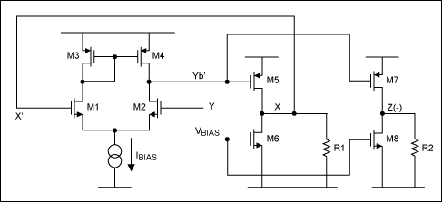
Figure 3. The current conveyor (CCII+) using an unbuffered amplifier.
The current from M5/M6 is simply mirrored by M7/M8, giving the output Z(-) of the CCII+.
The output impedance of Z can be improved by adding in a cascode to M7/M8 if necessary. One must be aware that to mimic the current successfully, the output impedance of X must match that of Z, i.e., the same transistor types and confirmation must be used on M5/M6 as on M7/M8.
The gain of the CCII is simply:

Converting from a CCII+ to a CCII-
Taking the bias point Yb' (Figure 3), simply add the extra connections as shown in Figure 4.

Figure 4. The current conveyor configured as a CCII-.
From Figure 4, if all transistor dimensions are the same and if Yb' (the bias point from Figure 3) is taken, then a current 2i is generated from M10 and M11. This is mirrored by M9 to give a current of 2i through M13. M12 provides a current of i and gives a current of -i through Z(+), thus giving a true CCII- output. There is a problem with this approach: the Z(+) now has an -i DC term instead of a +i term. Consequently, a 2i DC term needs to be added to the output of Z(+) to compensate for -i. Figure 5 below shows the addition.

Figure 5. The CCII- output with added DC bias.
From Figure 5, transistors M14 and M15 provide the appropriate current to compensate for the DC current taken by M13. (Note that M14 and M15 must match M12). Make the current through R3 equal to i(DC) - i'. Remember that R3 and R2 must match; any mismatch in their values will mean that their output DC values will differ.
The VBIAS Circuit
To create the necessary and appropriate voltage, VDCBIAS, that will maintain the DC currents in M14 and M15, then VDCBIAS (Figure 5) must have the same DC value as Node Yb' (Figures 4 and 5). To do this, simply mimic the front-end stage and take the DC value of the input signal as the input bias voltage into this stage (VINDC), as shown in Figure 6 below.

Figure 6. VBIAS circuit for the DC compensation circuit (Figure 5).
The only problem with this design is that another resistor (R4) is needed, and R4 must again match R2 and R3.
Simulation Results
Using the CCII+ as in Figure 3 and using a TSMC 0.18µm process with R1 = 1kΩ and R2 = 1kΩ, results in a gain of 1. The 3dB bandwidth of the device was 2.5GHz and had a gain of 0.972 with a power-supply reject ratio (PSRR) of 41dB.
These results were improved by using a cascode device to replace M5/M6 and M7/M8, which gave a bandwidth of 900MHz and an improved gain of 0.993. The PSRR was also improved at 51dB.
Related to this Article
Products
Single/Dual/Quad, 400MHz, Low-Power, Current Feedback Amplifiers
300MHz High-Speed Op Amp
Product Categories
Latest Media 21


