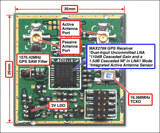
Figure 1. GPS reference design features the MAX2769
Important Design Features:
- Dual-Input Uncommitted LNA for Separate Passive and Active Antenna Inputs
- Integrated Active Antenna Sensor Which Can Autoswitch the Antenna Input
- The I and Q Channel-Select Filters Can Be Selected as Either Third or Fifth Order
- Provides 110dB Cascaded Gain and a 1.5dB Cascaded NF in LNA1 Mode
- The IF Output Is Adjustable in 63 Steps Between 0MHz and 12.5MHz
- Can Be Used in Preconfigured States that Do not Require Programming Through the 3-wire SPI™ Interface

Figure 2. Block diagram for the GPS reference design
Lab Measurements
Supply Current Summary
VCC = +3.0V, TA = +25°C
| Parameter | Test Conditions | Measurement | Unit |
| Operating Supply Current | Using LNA1 in Default and Low-Current Modes | 18 | mA |
Receive Summary
Operating conditions: VCC = 3V; TA = +25°C, Operating in default mode, PCB trace losses are included.
| Parameter | Test Condition | Measurement | Unit |
| LNA1 Power Gain | Default and Low-Current Modes | 18.6 | dB |
| LNA1 Noise Figure | Default and Low-Current Modes | 1.05 | dB |
| LNA1 Third-Order Input Intercept Point | Default and Low-Current Modes; LNA Input to Output. P1 = P2 = -30dBm; f1 = 1575MHz, f2 = 1567MHz | -1 | dBm |
| LNA2 Power Gain | Default Mode | 12.9 | dB |
| LNA2 Noise Figure | Default Mode | -2 | dBm |
| LNA2 Third-Order Input Intercept Point | Default Mode | -2 | dBm |
| Overall System NF | Using LNA1; PGA Gain is Maximum (CONF3[27:22] is 111111) | 1.6 | dB |
| Overall System NF | Using LNA2; PGA Gain is Maximum (CONF3[27:22] is 111111) | 3.1 | dB |
| IF Out Freq/Gain Range Thru System Using LNA1 | 1575.42MHz in, 4.092MHz out; Analog Output Mode | 59 -117 | dB |
| 4MHz Offset Rejection | 1579.42MHz in, third-order BPF; PGA Gain is Maximum (CONF3[27:22] is 111111) | 32 | dB |
| 4MHz Offset Rejection | 1579.42MHz in, fifth-order BPF; PGA Gain is Maximum (CONF3[27:22] is 111111) | 51 | dB |
| IF Passband 3dB Bandwidth | IF Filter Center Bandwidth 2.6MHz; Set Bit 4:3 of CONF1 Register to 00 | 2.9 | MHz |
| LNA1 Third-Order Input Intercept Point | Default and Low-Current Modes; LNA Input to Output. P1 = P2 = -30dBm; f1 = 1575MHz, f2 = 1567MHz | -1 | dBm |
Operating Characteristics

Figure 3. Input S11 of the MAX2769 LNA1. Measured by network analyzer at 1575.42MHz. The S11 is -10.4dB
Detailed Description
This reference design is a low-cost, single-conversion, low-IF GPS receiver. The design offers more flexibility and performance than its predecessors for a wide range of GPS applications such as mobile handsets, PDA's, embedded PCs, and automotive applications.
Related to this Article
{{modalTitle}}
{{modalDescription}}
{{dropdownTitle}}
- {{defaultSelectedText}} {{#each projectNames}}
- {{name}} {{/each}} {{#if newProjectText}}
-
 {{newProjectText}}
{{/if}}
{{newProjectText}}
{{/if}}
{{newProjectTitle}}
{{projectNameErrorText}}
Latest Media 21


