LTC6244 High Speed Peak Detector
Introduction
Peak detectors capture the extreme of the voltage signal at its input. A positive peak detector captures the most positive point of the input signal and a negative peak detector captures the most negative point of the input signal. Ideally the output of the peak detector circuit tracks or follows the input voltage until the extreme point is reached but holds that value as the input decreases. The ideal peak detector performs this function regardless speed of the input signal. The performance of the physical peak detector is limited by the bandwidth of the input signal. This paper will review the operation of the classic active peak detector circuit, highlight the parameters and components that limit the bandwidth; propose improvements to remove these limitations and present simulation results that compare the performance of the new circuits.
Classic Peak Detector
Figures 1 and 2 are depictions of two peak detector implementations. The circuit in figure 1 is that of a classic peak detector. The circuit in figure 2 addresses limitations of the classic peak detector. This discussion will review the operation of the classic peak detector, highlight the limitations of the circuit, explain how the improved circuit addresses these limitations and explore methods to further improve the circuit as shown in figure 3.


Figure 1. Classic Peak Detector
The circuit in figure 1 captures the peak value of the input voltage (IN). When IN is positive D1 is reverse biased, D2 is forward biased and no current flows in the feedback resistor R2. The output voltage (OUT) therefore tracks the input voltage (IN) because the outer feedback loop drives the inputs of U1 to a virtual short (V+ = V–). The output voltage tracks the voltage on capacitor C1 because U2 is configured as a voltage follower. C1 is charged to this voltage by the output current of U1 through the D2. R1 prevents the U1 from exceeding its short circuit output current and isolates U1 from the capacitance of C1 which prevents ringing or even oscillations. This state holds as long as the input voltage is positive and increasing.
The circuit in figure 1 changes state when the input voltage decreases. D2 is reverse biased when the input voltage decreases because the output of U1 (anode of D2) drops below the cathode voltage of D2 which is equal to the previous peak voltage stored on C1. The outer feedback loop is broken in this state and the output of U1 attempts to snap to the negative rail voltage. D1 is forward biased in this state and provides local feedback to U1 which clamps the anode of D2 at one diode drop below the input voltage. The hold state is maintained until the input voltage over comes the capacitor voltage which is equal to the output voltage. The D1 clamp reduces the transition time from the hold state back to the tracking state.
Speed is the major limitation of the classic peak detector circuit in figure 1. The output voltage cannot change any faster than C1 be charged. The speed at which C1 is charged is limited by the short circuit output current of U1, the forward voltage drop of D2, the commutation speed of D2 and the exponential rise due the time constant formed by R1 and C1.
Improved Peak Detector
The speed and error of the circuit in figure 2 better than that of the circuit in figure 1. The improvements are a result of addressing some of the limitations of the classic peak detector. Notice the rectifying diode has been changed to a Schottky barrier type. This change reduces the forward voltage drop which increases the initial charging current in through C1. In addition, the faster recovery time of the Schottky diode speeds the transition from the tracking state to the hold state. Moreover, the lower reverse recovery charge of the schottky diode reduces the pedestal error on the C1.
Although the voltage drop on the Schottky diode is lower it translates directly to the output because there is no outer feedback loop to compensate for it as there is in the classical circuit of figure 1. This circuit compensates for this diode drop by balancing it with a matching Schottky diode in the local feedback loop of U1. The two diode drops will mostly cancel if the matched diodes are similarly biased. R2 sets the bias current in D1 which will allow the voltage drop of D1 to cancel the voltage drop of D2 and minimize this error.
R5 and R6 form a resistive voltage divider that reduces the level of the input voltage. D3 clamps the input voltage at a diode drop below 0V which spares U1 and U2 of negative supply rails.

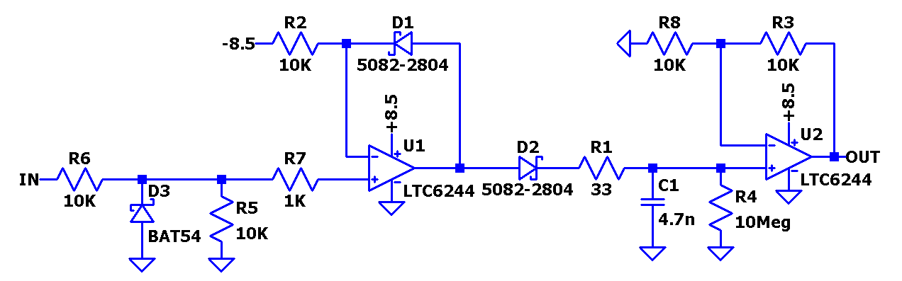
Figure 2. Improved Peak Detector
The LTC6244 is a dual high speed, unity-gain stable CMOS op amp that features a 50MHz gain bandwidth, 40V/μs slew rate, 1pA of input bias current, low input capacitance and rail-to-rail output swing. The 0.1Hz to 10Hz noise is just 1.5μVP-P and 1kHz noise is guaranteed to be less than 12nV/√Hz. This excellent AC and noise performance is combined with wide supply range operation, a maximum offset voltage of just 100μV and drift of only 2.5μV/°C, making it suitable for use in this application.
Current Boosted Improved Peak Detector
The circuit in figure 3 exploits the methods of the improved peak detector of figure 2 and adds a current boost to increase the C1 charging current. The current boosted peak detector replaces the matched diodes with matched NPN bipolar junction transistors (BJT). The circuit works exactly the same as the circuit in figure 2 but it charges C1 considerably faster.

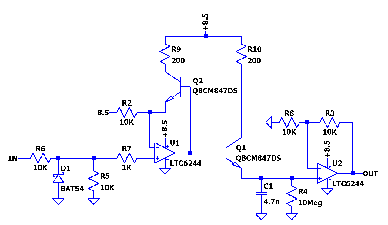
Figure 3. Current Boosted Improved Peak Detector
This topology offers some alternatives to the Schottky diode approach. The C1 charging current is increased by a factor equal to the current gain of the common collector BJT configuration. In addition, this topology presents a lower source impedance to C1. R3 is no longer necessary because the emitter follower has a greater current sourcing capacity than U2. As a result the charging time constant has been all but eliminated. The speed of the circuit in figure 3 is limited by the lesser of the bandwidth of the U2 and unity gain frequency of the emitter follower (fT). The voltage drop of the base-emitter junction of Q1 can be cancelled by the base-emitter junction of Q2 in the same manner as the D2 and D3 balance of figure 2.
Comparing the performance of the two high speed peak detectors, Figure 4 shows that both circuits perform equally well at 60 kHz and Figure 5 shows that the current boost modification increases the bandwidth.


Figure 4. Comparison at 60kHz

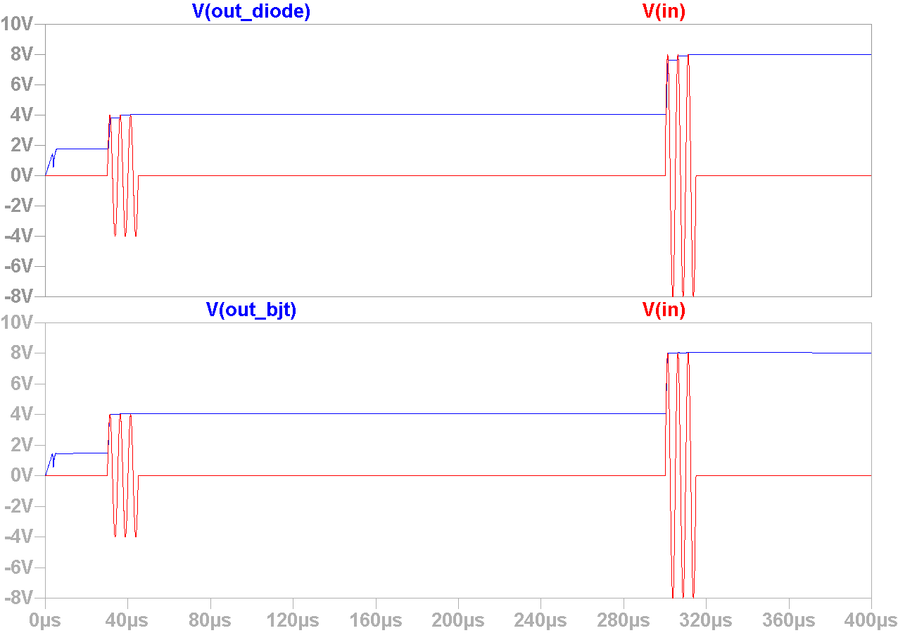
Figure 5. Comparison at 200kHz
Conclusion
The improvements of the current boosted peak detector of figure three are not without cost. However for applications where speed and precision matter, these circuit improvements could be well worth the additional power dissipation, part count and complexity.
About the Authors
Related to this Article
Products
Latest Media 21


