Abstract
This application note discusses the need for overvoltage protection in switches and muxes that connect to the rest of the system. The MAX4711/MAX4712/MAX4713 analog switches operate from 2.7V to 11V with integrated fault protection.Other methods of fault protection are discussed, along with their advantages and disadvantages.
The standard supply voltages for today's systems (unipolar 3.3V or 5V, or bipolar ±3.3V or ±5V) are usually the highest voltages available on a board. The board's input terminals may be exposed to voltages higher than the supply voltages. When power to the board is off, voltages may remain at the input terminals. The first element to be affected by overvoltage is often a multiplexer or a switch, so they must protect downstream circuitry.
The pass element in an analog switch contains one or more MOSFETs and has parasitic clamping diodes to the supply voltages for ESD protection. Figure 1 shows the equivalent circuit diagram for a closed analog switch. As long as V+ and V- are present and no input voltage exceeds those rails by the forward bias voltage of the clamping diodes (typically 0.6V), the diodes are reverse-biased and no current flows through them.

Figure 1. Equivalent circuit diagram for a closed switch.
Because improper supply-voltage sequencing can cause an overvoltage fault, many switches require that the most positive voltage be applied first and the most negative last. An input voltage with supplies off or an input voltage that exceeds a supply voltage causes current to flow through the clamping diodes. Those diodes can handle only a couple of milliwatts (depending on the IC's semiconductor process) before heat due to power dissipation damages the switch permanently.
Lower current levels can cause latchup-a condition in which the switch malfunctions and draws excessive current from the supplies. In most cases you can end the latchup without harming the switch by removing all voltages from the switch, but the board will not operate properly until you do.
External protection
A simple approach for protecting analog switches against latchup (Figure 2) adds high-current Schottky diodes, which have low forward-bias voltages of 0.3V maximum. If input voltage exceeds the supply voltage, the low Schottky voltage ensures that no current can flow through the clamp diodes, whose typical forward-bias voltage is 0.6V.
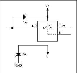
Figure 2. Latchup protection with external Schottky diodes.
The resulting latchup-free circuit has a downside (beyond the extra cost of two protection diodes). The Schottky diodes pass every voltage at least 0.3V higher than the supply voltage. That behavior is not a problem if the supply voltages are absent (V+ and V- at ground level) and the input voltage remains below the absolute-maximum rating for every part connected to V+ and V-.
But, the circuit provides no protection against overvoltage. If, for example, V+ = 5V and a fault voltage on the switch input is 8V, then V+ is pulled to approximately 7.7V—too high for most digital parts connected to V+. Even if V+ powers only the switch and the switch withstands the fault, high voltage may pass through the closed switch and damage downstream parts. Multiple-input switches require a Schottky diode from every input to V+, adding even more cost and board space.
The Figure 3 circuit provides good overvoltage protection for applications in which the input voltages are always off when supply voltages to the switch are absent. The forward-bias voltage VD (for a regular silicon diode) is typically 0.7V, so the zener voltage Vz1 must be selected to meet VD + Vz1 < V+. The same is true for the negative rail and Vz2: |VD + Vz2| < |V-|. Maximum voltage ratings for the diodes (zener and standard silicon types) must be chosen according to the maximum possible fault voltage.

Figure 3. Overvoltage protection with external diodes.
For a continuous-overvoltage fault (rather than a spike), a resistor placed between ground and the zener-diode connection limits current through that diode. The biggest disadvantage of such protection is a limitation on the input-voltage range of the switch. Because diodes differ greatly in bias voltage, min/max limits for the diode network can also vary greatly. When the network is dimensioned for a worst-case limit, the diode current can flow at a voltage much lower than the supply voltages, thereby eliminating the switch's rail-to-rail characteristic.
Resistors (kΩ-range) in series with the input channels can also give some protection by limiting the fault current that flows through the clamping diodes in a switch. Overvoltage can still damage parts downstream of the switch, however. The resistor dramatically increases on-resistance for the switch. Any variation of that resistance over temperature can corrupt the signal, as can leakage current from the switch flowing through the augmented on-resistance.
Internal protection
The first approach in integrating fault protection with an analog switch was for a certain type of multiplexer whose pass element consists of three MOSFETs in series, in the order n-channel/p-channel/n-channel. That architecture protects every signal path up to ±100V (Figure 4). The multiplexer's on-resistance, which increases rapidly for input voltages above the supply voltage, protects itself (and parts before and behind the multiplexer) by limiting the input current. Limiting the fault current prevents the fault from coupling into another channel.
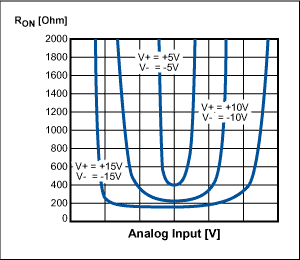
Figure 4. On-resistance vs. signal voltage for an older fault-protected switch.
The series-MOSFET approach also gives protection for the case in which no supply is present. Older parts like the MAX388 or HI-509A, on the other hand, operate only in the range ±4.5 to ±18V, come in large packages, have high on-resistance (minimum 350Ω, up to 3.5kΩ), and cannot pass input-signal voltages unless they are ~2V below the supply voltage.
The first step in addressing these problems for devices operating in the range 9V to 36V or ±4.5 to ±20V was the development of a new switch architecture, similar to the one described below as low-voltage fault protection. The new approach marks a major advance over the three-FETs-in-series technique by allowing rail-to-rail operation and lower on-resistance. Internal circuitry turns off the switch when it detects a fault, thereby preventing the fault from passing through the switch or mux to other circuitry.
Because only leakage currents flow into the switch or mux during a fault condition, the chip cannot be destroyed by power dissipation. Like their 3-FET predecessors, switches and multiplexers built with this new process and architecture eliminate fault problems when power is off by reverting to a high-impedance state. Such parts (including the MAX4511 switch and MAX4508 multiplexer families) are suitable for high-voltage systems requiring fault protection to ±40V, but not for common 3V and 5V systems. The parts mentioned are not specified for that voltage range, and their RDS(ON) with a 5V supply would be measured in thousands of ohms.
Low-voltage fault protection
Members of the newest fault-protected switch family are optimized for operation with a unipolar 3.3V or 5V supply, or with bipolar ±3.3V or ±5V supplies. They require no external protection, and they feature a low maximum on-resistance of 30Ω (±5V supply) or 100Ω (+3V supply).
As shown in Figure 5, these switches comprise an n-channel FET (N1) in parallel with a p-channel FET (P1), forming a low-value resistance from input to output. Input signals within the supply rails or that exceed the rails by no more than 150mV pass through the switch to the COM terminal, thereby allowing rail-to-rail operation.
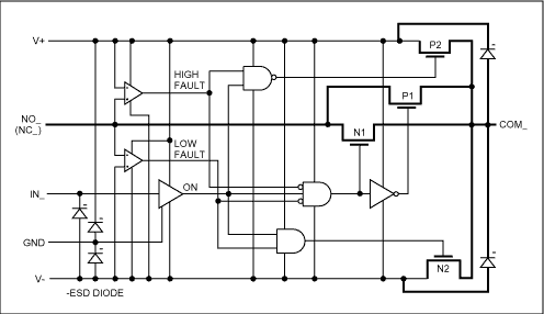
Figure 5. Block diagram of a low-voltage fault protected switch.
Two comparators monitor the input voltages by comparing them continuously with the supply voltages V+ and V-. When a signal on NO (normally open) or NC (normally closed) is between V+ and V-, the switch acts normally. When it exceeds the supply rails by about 150mV (a fault condition), the output voltage (COM) is limited to the supply voltage—at the same polarity and with the inputs at high impedance. That action is implemented by the fault comparators, which turn off N1 and P1. They also control the clamping FETs N2 and P2 as follows: if the switch is closed preceding a negative fault, N2 connects COM to V-. If closed preceding a positive fault, P2 connects COM to V+. If the switch is open preceding the fault, the output assumes a high impedance.
During a fault, the inputs assume a high impedance regardless of the switch state or load resistance. The maximum fault voltage on the inputs is limited by the absolute maximum ratings of the switches, which for the MAX4711 family is ±12V. If (for example) a MAX4711 device has a +5V supply, it is protected against fault voltages up to +12V on the positive rail and -7V on the negative rail (5V +|-7V| = 12V). The device provides fault protection for the input pins (NO and NC) when supply voltage is absent, and the protection is even better when off. For that condition, the fault voltage can approach ±12V for either rail.
The logic inputs (IN) are protected for positive faults up to (V-)+12V, but negative faults can exceed the negative supply by only a diode drop. The output terminal (COM) is not fault-protected, and (as described above) the COM voltage should not exceed either supply voltage by more then 0.3V.
Figure 6 displays the output voltage for a closed, fault-protected switch during input faults of both polarities. Typically, 200ns after the input voltage exceeds V+ (or V-) by approximately 150mV, the output (COM) equals the positive (or negative) supply voltage minus a drop voltage due to the FET. When the input fault returns within the supply rails, a delay of 700ns (typical) elapses before the output recovers and resumes following the input. That delay depends on the COM output's resistance and capacitance, and does not depend on the fault amplitude. Higher resistance and capacitance at COM increases the recovery time.
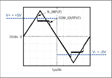
Figure 6. Input vs. output voltage during a fault condition.
Applications
Besides the obvious use of low-voltage, fault-protected switches in protecting the analog inputs of ATE and industrial equipment, those devices can ease the design effort and space requirements in many other applications as well.
To avoid powering down a rack of equipment, for example, many applications require the capability to insert an extension board into a live backplane. Though hot-swap controllers like the MAX4271 are available to limit a card's inrush current, its signal lines are not easily protected. If, for example, you insert the card into a backplane whose databus communicates via 5V TTL, the digital ICs (microcontrollers, ASICs, etc.) see 5V at their inputs before a supply voltage is applied. As mentioned earlier, that condition can cause latchup or damage the board.
Low-voltage, fault-protected switches between sensitive parts and the backplane connection (Figure 7) give the required over-voltage protection. The switches maintain their COM outputs in a high-impedance state until the card's supply voltage comes up and closes the switch connection to the backplane. The switch's protected (NO) inputs face the backplane, giving ±12V protection while power is off, and also protecting the card against overvoltage from the backplane when supply voltage is present. Note that the popular logic-bus switches from various vendors do not provide this sort of protection. They provide a higher allowable value for latch-up current than do standard CMOS parts, but they do not withstand continuous overvoltage.
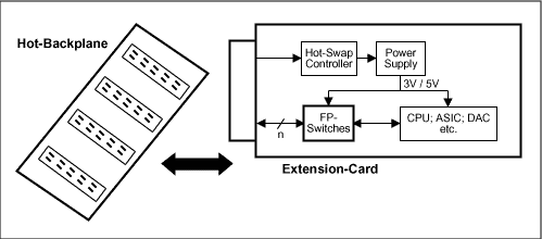
Figure 7. Hot-swapping backplane signals.
The low-voltage fault-protected switch in Figure 8 switches off the internal supply via a 9V battery (or two lithium coin cells in series, etc.) when it detects an external supply such as a wallcube (PS). Normally, the switch is supplied by the battery at pin 13. A low-voltage Schottky diode protects the non-rechargeable battery from being charged when an external supply is connected.
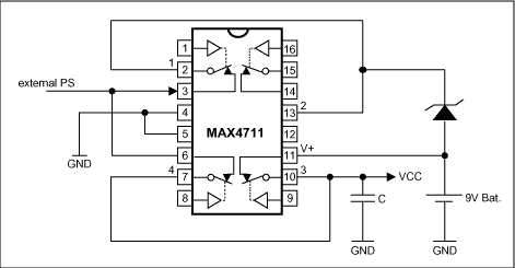
Figure 8. Battery switch off when external power supply is present.
A switch at pin 10 extracts VCC, which in most applications is conditioned by a voltage regulator after the switch. As soon as the board detects an external supply voltage, a microcontroller closes switches 1 and 4 and opens switch 3. The output capacitor C provides system power during the transition from switch 3 to switch 4. To protect the battery from damage, switch 3 must always be open when switch 4 is closed. When the external supply is removed, switches 4 and 1 open and switch 3 closes. Fault-protected inputs protect the switch when the external supply is higher than the battery voltage, when the battery is discharged and an external supply is connected, or when C is charged and the battery is removed.
Latest Media 21


