Intelligence at the Edge Part 2: Reduced Time to Insight
Read other articles in this series.
Reduced time to insights at the edge node can allow critical decisions to be made as soon as the data is available. With theoretically unlimited processing power and communications data, the full bandwidth from all edge node sensed information could be sent to a distant compute station in the cloud. Vast computations could be performed to mine the valuable details that are sought to make informed decisions. However, the limitations of battery power, communications bandwidth, and compute cycle intensive algorithms render that scenario merely a concept rather than a practical implementation.
In this multipart industrial IoT series, we will break down and explore the fundamental aspects of the edge node interpretation within the larger IoT framework: sensing, measuring, interpreting, and connecting data, with additional consideration for power management and security. The required data set from the edge node may need to merely be a discrete subset of the full wideband information. Similarly, data may be available for transmission only upon request. Energy efficient ultralow power (ULP) processing should also be a key aspect of any edge node implementation.
Smart Partition Paradigm Shift
The pioneer days of the industrial IoT and its precursor, machine-to-machine (M2M) communication, were largely defined by the role of cloud platforms as the primary application enablers. Intelligent systems have historically relied only upon cloud level capability for their insight. The actual edge sensor devices had been relatively unsophisticated. However, this old premise is currently being shaken up as low power computing capabilities at the edge node advance at a faster rate than those at the cloud.1 Edge nodes now offer the capability to sense, measure, interpret, and connect.
There is a smart partition paradigm shift underway from the connected sensor model to the intelligent device model. This is providing more available architecture choices and allowing organizations deploying the industrial IoT to enhance their physical assets and processes in unique ways. Edge computing analytics, also known as edge intelligence or interpretation, is driving this shift. Mass industrial IoT deployments rely on the availability of a diverse set of intelligent nodes that are secure, highly energy efficient, and easy to manage.
Edge Analytics
The highest quality sensed data can still be marginalized without careful attention to an application’s requirements within edge node analytics. Edge sensor devices may be constrained by energy, bandwidth, or raw computational power. These constraints propagate to protocol choices that can cut IP stacks down to minimal flash memory or RAM. This can make it challenging to program and there can be some sacrifice of the IP benefit.
Edge processing can be an analytic proposition as an approach to analyze data close to its source in addition to sending it to a remote server for cloud-level analysis. Moving the real-time analytics edge processing as early as possible in the signal chain reduces the payload burden down-stream and shortens latency. If the initial data processing can otherwise be done at the edge node, this will simplify the required data formatting, communications bandwidth, and eventual aggregation at the gateway to the cloud. Time sensitive feedback loops through close coupling to the sensor can provide immediate processing that provide for a more valuable informed decision.2
However, this requires advance intelligence about what specific information is valuable to expect from the sensed and measured data. It may also vary from edge node to edge node due to spatial separation or application differences. Event alerts, triggers, and interrupt detection can ignore a majority of the data to transmit only what is necessary.
Temporal Depreciation
The time value of money is the idea that a dollar today is worth more than a dollar sometime in the future. Analogously, there is a time constant for data. The time value of data means that the data you have sensed in this fractional second will not mean as much in a week, day, or even hour from now. Excellent mission critical IoT examples of this are heat surge sensing, gas leak detection, or sensing catastrophic machinery failure that requires immediate action. Time sensitive data value decay starts at the point of interpretation. The longer the latency to effectively interpret your data and take action, the less valuable the decision will be. In order to solve the temporal depreciation riddle within the industrial IoT, we must gain insights further ahead in the signal chain.
Processing algorithms within the edge sensor node can be used that filter, decimate, tune, and refine the sampled data down to the minimum required subset. This requires first to define the narrow data of interest. Adjustable bandwidth, sample rate, and dynamic range help establish this baseline in the analog domain of the hardware at the onset. By using the required analog settings, the sensor will target only the needed information and provide a shorter time constant to quality interpreted data.
Digital postprocessing at the edge can further focus the data of interest. Frequency analysis of the data at the edge sensor can make early decisions about signal content before the information leaves the node. Performing fast Fourier transforms (FFTs), finite impulse response (FIR) filtering, and using intelligent decimation are some high order computational blocks that narrow the scope of the sampled data. In some cases, only an incremental breadcrumb of pass or fail information is needed to be transmitted out of the edge sensor node after dramatically reducing the full bandwidth of data.
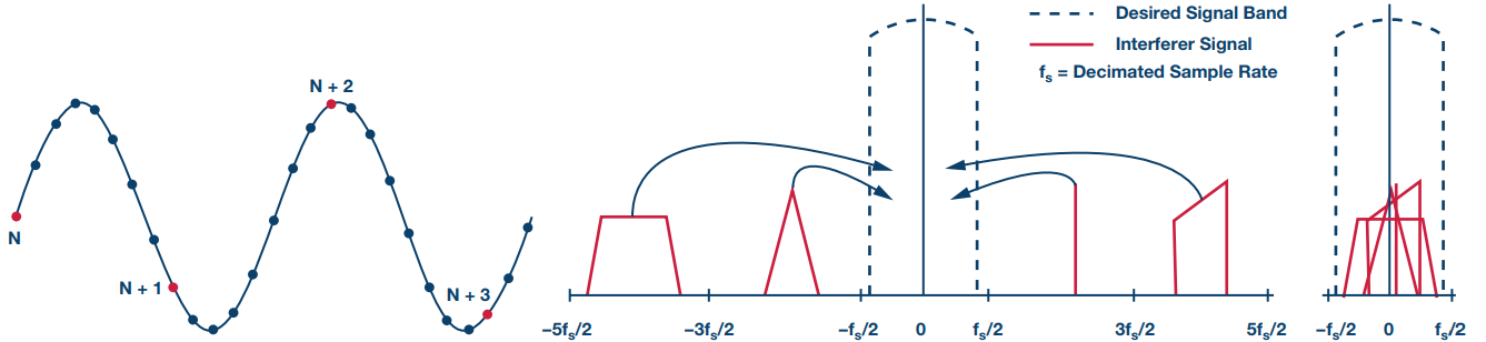
In Figure 1, we can see that without a front-end analog filter or a digital postprocessing filter, a simple signal with decimation by 8 (left) will alias new unwanted signals (center) to frequency fold into the new desired signal band (right). Digital postprocessing, with a digital signal processor (DSP) or microcontroller unit (MCU), using a half-band FIR low-pass filter as a companion to decimation, will help prevent this issue by filtering the interfering aliased signals.

Processing for Edge Node Insights— Smart Factory
A leading industrial IoT application is a solution for factory machine condition monitoring. The intent of the solution is to identify and predict machine performance issues in advance of failure. At the edge sensor node, a multiaxis high dynamic range accelerometer monitors vibration displacement at various locations on industrial machines. The raw data can be filtered and decimated for frequency domain interpretation within a microcontroller unit. An FFT compared against known performance limits can be processed for testing against pass, fail, and warning alerts downstream. Processing gain within the FFT can be achieved through FIR filtering to remove wideband noise that is otherwise outside the bandwidth of interest.
The edge node processing is an important component in machine condition monitoring. The full bandwidth of sampled data can provide a significant bottleneck for the aggregation at the wireless gateway. Consider that a single machine may have many sensors and hundreds of machines may be monitored concurrently. The filtering and intelligent decision making within the microcontroller unit offers a low bandwidth output to the wireless transceiver without the need for intensive filter processing at the cloud.
Figure 2 shows a signal chain for machine condition monitoring where an accelerometer sensor measures a displacement vibration signature. With postprocessing at the edge sensor node, frequency analysis can be done within a narrow bandwidth of interest by filtering and decimating the sampled data ahead of FFT computation.


During FFT computation, similar to a real-time oscilloscope, the processing can be blind to new time domain activity until the FFT is complete. An alternate time domain path in a second thread may also be used to prevent gaps in the data analysis.
If mechanical signature frequencies of interest are known precisely, the sample rate of the ADC and FFT size within the microcontroller unit can be planned such that the maximum amount of energy falls within the width of a single histogram bin. This will prevent the signal power from leaking across multiple bins, diluting the precision of the amplitude measurement.
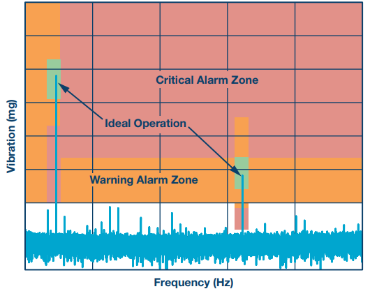
Figure 3 provides an example of an FFT where specific predetermined zones are interpreted within the edge node MCU for more than one observed mechanical component. Bin energy that peaks within the required green zone represents satisfactory operation, while the yellow and red zones indicate warning and critical alarms respectively. Instead of transmitting the full sensor bandwidth, a lower data rate alarm or trigger breadcrumb can alert the system of an excursion event within the zones of interest.

Dynamic Range, Notation, and Precision
There are several choices available for the computational horsepower of the edge analytics. Many options are available for processing algorithms, from a simplistic MCU that provide limited controls, more complex MCUs that are a sophisticated system on a chip (SoC), to powerful multicore digital signal processing. The processing core size, a single- or dual-core operation, instructional RAM cache size, and fixed vs. floating-point needs are typical technical considerations. Often there is a trade-off between the power budget available on the node and the computational requirements of the application.
For digital signal processing, two categories designate the notation format used to store and manipulate numeric representations of the sensor node data: fixed point and floating point. Fixed point refers to the manner in which numbers are represented with a fixed number of digits after and sometimes before the decimal point. DSPs using this method process integers such as positive and negative whole numbers using a minimum of 16 bits with 216 possible bit patterns. In comparison, floating point uses rational numbers with a minimum of 232 possible patterns.3 DSP using a floating-point computation method can process a much wider range of values than fixed point with the ability to represent very large or small numbers.
Floating-point processing assures that a much larger dynamic range of numbers can be represented. This is important if large sets of sensor node data are to be computed where the exact range may be unknown in advance of sensing. Additionally, since every new computation requires a mathematical calculation, rounding or truncating is an inherent result. This creates quantization errors, or digital signal noise, within the data. A quantization error is the difference between an ideal analog value and its digital representation that is the nearest rounded value. The larger the quantization gap between these values, the more pronounced the digital noise will be. Floating-point processing yields greater precision than fixed-point processing when accuracy and precision are important to the interpreted sensor data.
Performance
Firmware designers should implement a computation application with the greatest efficiency, as the speed with which operations execute is critical. Therefore, it is important to delineate the processing requirements for data interpretation to determine whether fixed or floating-point computations are required for maximum efficiency.
It is possible to program a fixed-point processor to perform floating-point tasks and vice-versa. However, this is highly inefficient and will impact processing performance and power. Fixed-point processors shine where they are optimized for higher volume general-purpose applications that do not need intensive computation algorithms. Floating-point processors conversely can leverage specialized algorithms for ease of development and greater overall precision.
While not high in performance, the number of supported GPIO pins within the processor can provide a secondary selection criteria. Direct support of the right control interface for the sensors of interest, such as SPI, I2C, SPORT, and UART, reduce system design complexity. The core processing clock speed, number of bits per execution, amount of embedded instruction RAM available for processing, and memory interface speed will all impact the capability of the edge node processing. Real-time clocks help time-stamp data and allow alignment of processing across multiple platforms.
Processing computational power is often defined in MIPS or MMAC. MIPS is the number of million instructions that can be executed within a second. MMAC is the number of single precision floating-point or fixed-point multiply-and-accumulate 32-bit operations that can be executed in millions per second. MMAC performance values increase respectively by a factor of 2× and 4× for 16-bit and 8-bit operations.3
Security
While full security of the industrial IoT spans each and every system, transmission, and data point access, microcontrollers, and DSP offer internal security features. The advanced encryption standard (AES) provides a means for adding security on a wired link, such as UART/SPI, or a wireless link. In the case of wireless RF communication, AES encryption is performed prior to payload transmission via the edge node radio. The receiving node correspondingly performs the converse decryption. Electronic code block (ECB) or cipher block chaining (CBC) are typical modes of AES.4 A security key of 128 bits or larger is often preferred. A true random number generator is used as part of the security computation within a processor. The details of these schemes will be described in more detail in future industrial IoT articles for a more comprehensive security approach.
Single or Dual Core
Raw processing power will always be in demand. Efficient raw processing power is even better. Multicore MCUs and DSPs can provide additional computational power for algorithms that specifically benefit from intensive parallel processing. However, the need to often process disparate data is also increasing. This has given rise to a class of multicore microcontrollers that bring together two or more cores with specific, but different, functional strengths. Commonly referred to as heterogeneous or asymmetric multicore devices, they often feature two cores with very different profiles.
An example of an asymmetric MCU could feature both an ARM® Cortex®-M3 and Cortex-M0, which communicate using an interprocessor communication protocol. This allows the M3 to focus on heavy digital signal processing tasks while the M0 implements the lower intensive control aspect of an application.5 The concept allows simpler tasks to be offloaded onto the smaller core. The partitioning maximizes the processing bandwidth of the more powerful M3 core for compute-intensive processing, which is really at the heart of coprocessing. The intercore communication uses a shared SRAM with one processor raising an interrupt for the other to check. This alert is acknowledged when the receiving processor raises an interrupt in response.
Another benefit of heterogeneous multiple core MCUs is to overcome the speed limitations of embedded flash memory. By partitioning tasks in an asymmetric way across two small cores, the full performance of the cores can be accessed while still utilizing low cost embedded memory. The cost of implementing embedded flash often dictates the cost of an MCU, thus the bottleneck can be effectively removed. Balancing the processor demands within the available power budget can be a key part of the industrial IoT edge sensor node design.5
Balance of Power
Many industrial IoT edge sensor nodes must be able to operate for years on the same small form-factor battery, even when energy harvesting is possible. ULP operation will be a key parameter for these nodes, and components must be selected that minimize the real-world current consumption of the node.6
Many MCUs that are best suited for the industrial IoT are based on the ARM family of Cortex-M embedded processors, which are targeted for low power MCU and sensor applications.7 These range from the Cortex-M0+, optimized for power efficient simpler applications, to the Cortex-M4, for complex high performance applications requiring floating-point and DSP operations. Higher processing cores can be used at the expense of low power.
The ARM CPUs provide a starting point in terms of code size, performance, and efficiency. But when it comes to the MCU’s actual current consumption in active or deep sleep modes, many ultralow power capabilities are entirely up to the MCU vendor. Active current consumption can be heavily influenced by process technology choices, caching, and the overall architecture of the processor. MCU sleep current and the peripheral functionality available while the CPU is sleeping are mostly influenced by the MCU’s design and architecture.
The EEMBC, an industry alliance, develops benchmarks to help system designers select the optimal processors by helping them understand the performance and energy characteristics of their systems. The ULPMark™-CP score reported for each device is a calculated single-number figure of merit. Scores for each of the individual benchmarks within this suite allow designers to weight and aggregate the benchmarks to suit specific application requirements.8
The power budget for the sensor edge node will directly correlate to its processing capacity. If the power budget does not agree with the processing needs of the edge node analytics, a trade-off may need to be made. Performance efficiency can impact the power efficiency of the sensor edge node. A typical power consumption metric for microcontrollers is to specify the amount of active current used per MHz of computation. As an example, for an MCU that is based upon the ARM Cortex-M3, the current can be in the tens of μA per MHz.
Duty Cycle
Power consumption minimization for the edge sensor node is often based on two factors: how much current the node consumes while it is active and how often it must remain active to sense, measure, and interpret. This duty cycle will vary based on the type of sensor and processor used in the node as well as requirements of the algorithm.
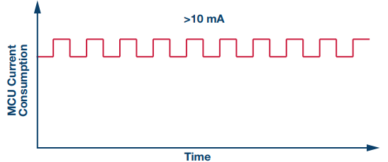
Without consideration for the MCU current consumption, a mostly active state will consume considerable power within the edge sensor node and reduce the lifetime of a battery-powered application to mere hours or days.

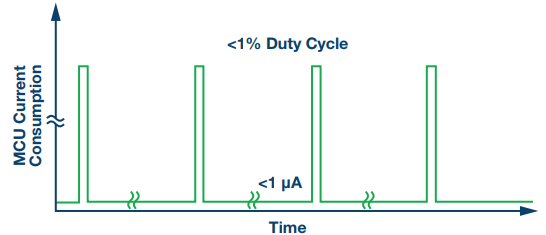
Significant energy savings are achieved by duty cycling the components within the node, making sure they are active only when strictly needed. The MCU is rarely turned all the way off. It must be specifically architected for low energy operation in order to enable the MCU to keep full control of the edge sensor node while consuming as little energy as possible. Minimizing MCU current consumption is all about making the MCU sleep as often as possible while still allowing it to execute its critical tasks when they are needed.
Keeping the MCU operating within a low power hibernate mode for a mostly inactive state, only to be active during a short duty, can extend battery life for the edge node to many years.

Many edge node sensing solutions within the industrial IoT may not be required to process a continuous uninterrupted stream of data. Ignoring data from known out-of-bounds conditions using interrupt event thresholds can reduce the processing power. To conserve both power and bandwidth, a predictable on duty cycle may be known in advance. Additionally, a variable duty cycle based on the state of sensed information can trigger either an active or reduced power state.
The response time and power consumption, both turn-on and turn-off, of the microcontroller or DSP can be important design considerations to low bandwidth applications. For example, the transmission of data from a temperature and light sensor may be reduced significantly during periods of inactivity within a building. This allows longer sleep times at the sensor node and far fewer transmissions of information.
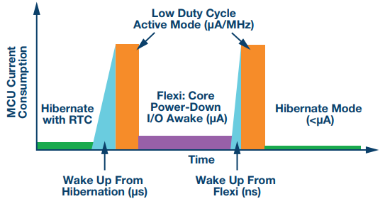
To provide a rapid reaction, many microcontrollers provide various states of low power operation in additional to being fully active such as sleep, flexi, hibernate, and full power-down. Each mode will power down various internal computational blocks for power efficiency when not needed, often changing the current requirements by several orders of magnitude. The trade-off for this power benefit is that there will be some minimum finite response time to transition to full activity. In a hybrid configuration known as flexi mode, the computation core is in sleep mode while the peripheral interfaces remain active. Hibernate mode can provide SRAM data retention with the option to still allow the real-time clock to remain active.
The detailed MCU power consumption vs. timing diagram in Figure 6 shows the impact of each low power MCU mode, transition time, and duty cycle. Using low power states when the MCU is not active is key to keeping within a low power sensor node budget.9

Sensor Fusion
Advanced analog microcontrollers provide a full mixed-signal computational solution. A front-end analog mux with an embedded precision analog-to-digital converter (ADC) allows for a more advanced sensor fusion approach. Multiple sensor inputs can be sent to a single microcontroller ahead of digital processing. On-board digital-to-analog converters (DACs) and microcontroller feedback to other nearby equipment permits a rapid feedback loop. Other embedded circuit blocks such as a comparator, band gap reference, temperature sensor, and phase-lock loop provide additional algorithm flexibility for a multi sensor edge node.10

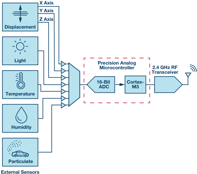
Analog signals from multiple sensors can be sent to a single precision analog microcontroller. Algorithms within the microcontroller intelligently can combine the information in a process known as a sensor fusion.
An example of this type of edge node processing is within an outdoor pollution monitor. In such an application, data from multiple inputs, including gas, temperature, humidity, and particulate sensors, are fused and analyzed within a single processor. From this information, processing can be done to generate pollution figures based on calibration and compensation known only at the local sensor node. This calibrated data can then be sent to the cloud for historical analysis. In some cases, unique one-time commissioning may be needed to configure each sensor node for its particular environmental offsets.9
Analog Devices has invested in a ULP platform with significant innovation in sensors, processors, and strong feature sets within power efficient modes. The recently announced ADuMC3027 and ADuMC3029 family of microcontrollers delivers the performance of a 26 MHz ARM Cortex-M3 core with an operating current specification of less than 38 μA/MHz in active mode and 750 nA in standby mode. This efficient power local processing capability reduces the overall system power while substantially reducing the need to send data through the network for analysis.9
Analog Devices offers a wide variety of MCU and DSP engines that can help intelligently capture and process IoT data that is destined for the cloud. The ADuCM36x family offers an ARM Cortex-M3 processing core with integrated dual Ʃ-Δ ADCs. Analog Devices’ SHARC® digital signal processor family brings real-time floating-point processing performance to many applications where dynamic range is key.4
A next-generation Cortex-M33 processor is based on the ARMv8-M architecture with proven ARM TrustZone™ technology that helps secure trusted applications and data using hardware built into the processor. As the world becomes increasingly connected, securing every node is critical to extending the growth of IoT adoption.
About the Authors
Related to this Article
Industry Solutions
Resources
Latest Media 21