Inductor Choice Yields Performance Tradeoffs in DC-DC Converters
Abstract
Cost, size, resistance, and current capability drive the choice of inductor for most step-down DC-DC switching converters. Many such applications specify the inductor value shown in the switching converter's data sheet or evaluation kit, but those values are usually specific to application or performance criteria. Portable applications, for instance, uphold size as the main consideration because such little space is available. The following discussion evaluates inductors for efficiency, noise (output ripple), and transient response using an evaluation kit designed for the MAX8646 switching converter.
The MAX8646 evaluation kit (EV kit) shown in Figure 1 includes a 0.47µH inductor that combines good efficiency with a quick response to load transients. Lower inductor values further improve transient response, while higher values provide better efficiency at the expense of transient response. Alternate inductors discussed in this article (Table 1) were chosen to fit the PCB footprint on the EV kit circuit board, and to require minimal (if any) changes to the circuit (as seen in the Appendix).
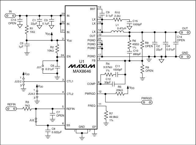
Figure 1. This schematic shows EV kit circuitry for the MAX8646 step-down switching regulator.
| Manufacturer | Series | Inductance (µH) | Current Rating (A) | Dimensions (mm x mm x mm) |
|
| Toko® | FDV0620 | 0.2 | 4.5 | 16.2 | 6.7 x 7.4 x 2.0 |
| 0.47 | 8.3 | 11 | |||
| 1.0 | 18 | 7.7 | |||
| FDV0630 | 0.47 | 4.6 | 16 | 7.0 x 7.7 x 3.0 | |
| 1 | 10 | 9.1 |
Size Considerations
The two series of inductors in Table 1 provide different core sizes. Their footprints are similar, but the FDV0630 series inductors are 1mm taller. The greater height makes possible a shorter length of copper wire—using a larger wire diameter or fewer turns, or both.
Inductors of 0.2µH and below give poor efficiency, so smaller values were not considered. Smaller values also give higher peak currents, which must remain below the MAX8646 minimum specified current limit to avoid loss of regulation. On the other hand, inductor values greater than 1µH are not suitable either. An evaluation of the 0.47µH and 1µH values makes these tradeoffs clearer. Note that the larger FDV0630 series inductors have the same values and footprint as those of the FV0620 series, but offer lower resistance and higher current ratings. A detailed comparison of the size, material, and permeability of inductor cores is beyond the scope of this discussion, but many articles on these topics are available from inductor manufacturers.
Core Considerations
Inductors of the FDV series from Toko have iron-powder cores, which offer good temperature stability and lower cost than most other core options. Other options are molypermalloy powder (MPP) toroids,
Performance Evaluations and Efficiency Comparisons
A comparison of efficiencies for the various inductors operating in the Figure 1 circuit (Figure 2) shows that 1µH inductors offer the best efficiency for output currents less than 2A, and that the 0.2µH inductor is least efficient below 3A. Comparing same-value inductors, the lower DCR associated with larger size (FDV0630 series) provides 0.5% to 1% better efficiency over the entire range of output current.
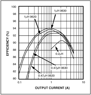
Figure 2. Efficiency vs. output current for various inductors operating in the Figure 1 circuit.
For 0.47µH and 1µH inductors of the FDV0620 series, note that there is a crossover in the efficiency curves near 2A. The 1µH inductor has higher efficiency below 2A, but the 0.47µH inductor is higher above 2A. Greater series resistance in the 1µH inductor causes this efficiency difference.
Comparison of Switching Waveforms
Another performance tradeoff can be seen (Figures 3 and 4) in the typical waveforms for inductor current, inductor voltage (pins 14 through 16), and output voltage ripple. The smaller valued FDV0620-0.47µH inductor used in Figure 3 produces higher peak current. Output-voltage ripple is just under 18mV peak-to-peak, but a FDV630-1.0µH inductor (Figure 4) produces just over 12mV peak-to-peak. Peak currents charge the output capacitor and supply load current. Because the capacitor's ESR sees higher currents in and out, it produces higher output-voltage ripple. If necessary, you can reduce this ripple by substituting a larger output value capacitor.
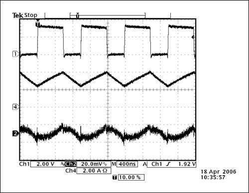
Figure 3. Waveforms from the Figure 1 circuit operate with 3.3V input, 1.8V output, 3A load current, and a 0.47µF inductor of the FDV0620 series. CH1 = VLX, CH4 = ILX, and CH2 = VOUT. (CH1 is the voltage at pins 14 through 16, not the voltage across the inductor.)
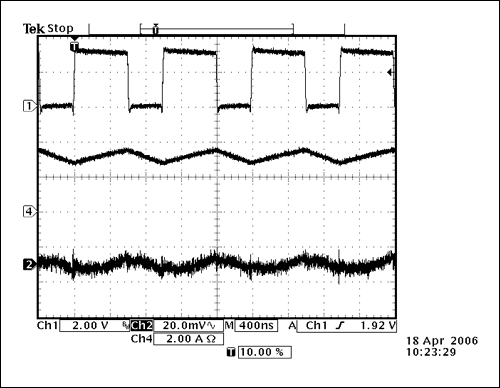
Figure 4. Same as Figure 3, but with a 1µF inductor of the FDV0620 series.
Load-Transient Comparisons
Different inductors offer different load-transient responses. (The IC and compensation network also contribute to this response.) Typical switching regulators include internal compensation and usually specify an allowed range of inductor values. The MAX8646 employs external compensation, however, which allows more design flexibility.
Figures 5 and 6 show the load-transient responses for the Figure 1 FDV0620-0.47µH and FDV0620-1µH inductors, which operate with load steps from 2A to 5A and back to 2A. In Figure 6, the external compensation was modified to accommodate the 1µH inductor value. Referring to Figure 1, three components were changed for that accommodation: C10 = 1000pF, R4 = 5.9kΩ, and R6 = 316Ω. Note that the output-voltage overshoot in Figure 5 is less than that of Figure 6. No differences in response were measured for same-valued inductors from the FDV0620 and FDV0630 series.
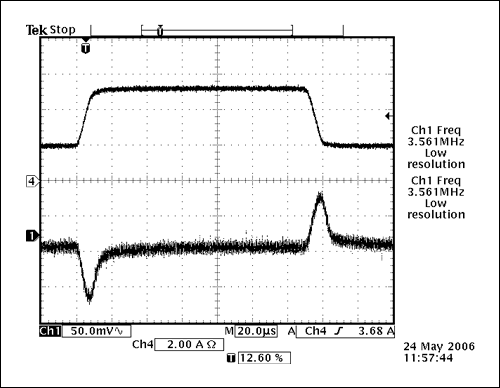
Figure 5. This load transient obtained from the Figure 1 circuit operates with 2A to 5A output current, 1.8V output, 3.3V input, and a 0.47µH inductor of the FDV0620 series. CH4 = IOUT, and CH2 = VOUT
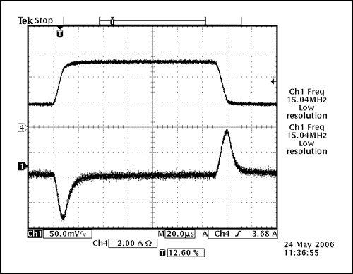
Figure 6. Same as Figure 5, but with a 1µF inductor of the FDV0620 series.
Theory of Operation
Having presented the results measured for a selection of inductors, we now sketch the theory of their operation. The following equation neglects the parasitic characteristics found in a real inductor, but it provides a good understanding of inductor operation.

The high-side MOSFET is on, and connects the inductor to the input supply voltage during the inductor charge time (tON). You can substitute tON = ΔT for dt and (VIN - VOUT) for V, and then calculate ΔI (for di) after choosing the inductor value. Table 2 shows the ΔI values associated with the inductors discussed in this article (based on the Figure 1 circuit). Other Figure 1 conditions supporting Table 2 are VIN = 3.3V, VOUT = 1.8V, and ΔT = D × T, where D is the duty cycle (VOUT/VIN) and T is the period of the switching frequency (1/fS).
| Inductor (µH) | ΔI (A) |
| 0.47 | 1.74 |
| 1 | 0.818 |
The midvalue of di/dt (ΔI/ΔT) equals IOUT, so the peak current equals IOUT plus ΔI/2. You can see how a smaller inductance value causes a higher peak current for the same load current.
DC Resistance (DCR)
Power loss across the IC and inductor can be derived from the efficiency curves. Choosing an output current of 1A and referring to the FDV0620-0.47µH in Figure 2, the efficiency is 92.5%. Power out is 1A at 1.8V, or 1.8W, so the power in is 1.8/0.925 = 1.946W. The total power loss is therefore PIN - POUT = 0.146W. The main sources of loss are the inductor DCR, the MOSFET RDS(ON) (conduction), and switching losses. IOUT² × DCR equals power loss across the inductor.
The DCR power loss of 8.3mW for the FDV0620-0.47µH at 1A output current (see Table 3) is 5.7% of total losses. For IOUT = 4A, PIN = 8.1W, and POUT = 7.2W (efficiency = POUT/PIN = 88.9%), the total loss is PIN - POUT = 0.9W, so the DCR power loss of 132.8mW for the FDV0620-0.47µH at 4A is 14.7% of total losses. The IOUT2 effect causes a higher DCR loss at higher output currents.
| Series and Value | PDCRLOSS at IOUT = 0.5A (mW) |
PDCRLOSS at IOUT = 1A (mW) |
PDCRLOSS at IOUT = 4A (mW) |
| FDV0620-0.47µH | 2.1 | 8.3 | 132.8 |
| FDV0630-0.47µH | 1.15 | 4.6 | 73.6 |
| FDV0620-1µH | 4.5 | 18 | 288 |
| FDV0630-1µH | 2.5 | 10 | 160 |
Conduction Losses
Conduction losses are a function of inductor current (IOUT), duty cycle (D), and the DC-DC converter switch RDS(ON):
PCONDM = ILX² × RDS(ON) × D
High-side conduction losses:
For 1A output current, PCOND = 1² × 0.022 × 1.8V/3.3V = 12mW.
For 4A output current, PCOND = 4² × 0.033 × 1.8V/3.3V = 288mW.
Low-side conduction losses:
For 1A output current, PCOND = 1² × 0.022 × (1 - 1.8V/3.3V) = 10mW.
For 4A output current, PCOND = 4² × 0.033 × (1 - 1.8V/3.3V) = 240mW.
The RDS(ON) values used at 1A are typical room-temperature measurements. However, at higher currents, the MOSFET operates at higher temperatures. Because RDS(ON) should be adjusted for the higher temperature, we use 33mΩ at the 4A output current.
Switching Losses
Switching losses occur during switch turn-on and turn-off, and also as a result of current flow that charges and discharges the MOSFET's gate capacitance. For short intervals during turn-on and turn-off, the voltage is high and the current ramps up before the voltage falls. The following equations approximate switching power loss in the switches:
PSW = ½V × IOUT × tSW × fSW
where tSW is the turn-on or turn-off time, and fSW is the converter's switching frequency. For an output current of 1A:
PSW = ½ × 3.3V × 1A × 5ns × 1MHz = 8.24mW
You cannot easily measure tSW in this example, because the MAX8646 switches are internal, and they share a common connection at LX (pins 14 through 16). Rise and fall times at LX before and after the dead time are roughly 5ns each.
The power loss calculated above is for either turn-on or turn-off, but not both. Because tSW values are the same for rise and fall at LX in this example, you should multiply that number by 4. If the MOSFET is external and can be measured, then you can make individual calculations with more accurate results. For the 0.47µH inductor at 1A output current, on and off switching losses are roughly 32.96mW each.
Conclusion
The tradeoffs of selecting the inductor for a pulse-width modulation (PWM), voltage-mode switching regulator are easily determined. Larger inductance values provide lower peak currents and lower losses, which improves the efficiency. Smaller inductors usually give a lower efficiency, but they provide a quicker response to step changes in line or load. A larger core size in an otherwise similar inductor offers a lower DCR for the same inductance value, which enables better dynamic performance with lower DCR loss. In any case, you should always conduct bench tests before finalizing a circuit.
Appendix—Hardware Description
The MAX8646 EV kit (Figure 1) enables customer evaluation of the MAX8646 6A step-down converter. The kit generates selectable output voltages with load currents as high as 6A, powered by input voltages in the 2.35V to 3.6V range. The MAX8646 in this circuit operates at a switching frequency of 1MHz and provides high efficiency with the components shown in Figure 1.
The MAX8646 step-down switching regulator features PWM for output-voltage regulation and low-RDS(ON)
A similar article appeared on the Power Management DesignLine web site on June 5, 2006.
Related to this Article
Products
Evaluation Kit for the MAX8646
PRODUCTION
6A, 2MHz Step-Down Regulator with Integrated Switches
Product Categories
Latest Media 21


