Abstract
This application note describes how to implement an ultra-low-power, low-cost, two-port USB 2.0 switch with the MAX4906EF. This circuit adds a 2:1 switch to the USB design with nearly zero added current, permitting the reuse of a single transceiver for several sockets.
Introduction
Many USB systems require multiple ports, but do not need all ports to be active at the same time. For example, in a consumer product with both front- and back-panel ports for a memory drive, it may be perfectly acceptable to permit only one port to be used at a time. In this case, a USB switch is an ideal solution because it requires very low (almost zero) power, and does not introduce another level between the device and the root complex.
This application note describes how to implement a USB 2.0-compliant* switched system using the MAX4906EF.
USB 2.0 Compliance
USB 2.0 (Hi-Speed USB) requires a data rate of 480Mbps, and that the system pass an eye diagram test to assure compliance. The eye diagram simultaneously displays the D+ and D- traces from a valid source, and resembles a human eye. Figure 1 provides a template of the eye pattern required by the USB 2.0 specification. If the output of the device passes the eye diagram test, the system is in compliance.*
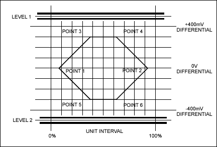
Figure 1. Illustrates the eye pattern required by the Universal Serial Bus Specification Revision 2.0 (refer to Figure 7–13 in the specification).
If we assume that the system under scrutiny has a switch on board and a connector at the output, then the signal must be outside the eye. The eye opening is ±400mV, and permits a small loss of up to about 2dB. The MAX4906EF USB 2.0 switch has a low, 0.5dB frequency loss, so there is no problem with the eye opening.
The next issue is the bandwidth of the system. The sloped lines, left and right, give the permissible rise and fall times for the system. The D+ (noninverted data) signal has to pass without touching the hexagon. Since the system is basically an RC filter, it would first appear that this is easy to calculate. If we assume the system is perfectly matched to 45Ω (per the USB specification) and double-terminated, the signal looks like the very familiar:
V = V0 × (1 - e-t/RC), where R = 22.5
The D+ display needs to show the curve from V = 50% to V = 100%; per the specification, the left-most point is 7.5% UI (unit interval) or (0.075) × 2.08ns, or 156ps.
When used on an ideal board, the MAX4906EF meets these requirements, passing the eye pattern test with ease.
Capacitance Problems Introduced by Nonideal Boards
However, problems may arise when a system designer attempts to integrate the MAX4906EF onto a nonideal board. Often, the designer does not have a say in what type of board to use; this is dictated by the buyers and other boards used in a system. If the designer were to try to put special constraints as to the materials, the thickness of the layers, the dielectric constant of the boards, it would either cost too much, or he could not get it done in time. The designer usually has no choice, then, but to use the style of board that other users in his company are using.
Ideally, the board can be used as an excellent transmission line. If the thickness can be controlled, and if the width of the lines and spacing can be completely specified, then it is fairly easy to get the traces to be near-ideal transmission lines. Typically, the very difficult high-frequency boards have unique requirements: the lines need to be separated by 4 mils (0.1mm) thickness, and 5 mils (0.125mm) wide, separated by 5 mils. Nearly all PCIe® boards are built using FR4 material with a dielectric constant of ≈4.4. It is not feasible to try to get a true 90Ω to 100Ω balanced transmission line, unless the layers are very thin or the traces very wide.
The board designer is usually stuck with the board constraints and a maximum of four layers. If the layers are equally spaced, then the dimensions are fixed. Almost all board material is 62 mils (1.5mm), making the insulating thickness ~18.6 mils (0.47mm). With normal spacing between the traces (10 mils to 20 mils), the characteristic impedance of the lines is much higher than desired, as much as 180Ω (nearly double the desired impedance). If the lines are short (< ¼λ), then these lines add capacitance in the system.
Implementing a USB 2.0-Compliant* Switched System
Designed with robust input structures, the MAX4906EF provides ±15kV HBM (Human Body Model) ESD (electrostatic discharge) protection. Even though these structures add to the capacitance of the part, they eliminate the need for an external diode or other devices for ESD suppression. Thus, they reduce total system cost and, very likely, capacitance, since no other parts are needed.
We now know that the MAX4906EF passes the eye pattern test on an ideal board, but with more standard boards, it has a difficult time with the eye opening. The MAX4906EF is low cost, has high immunity to ESD events, passes nearly all the requirements for USB 2.0, and is backwards compatible with USB 1.1 (low/full speed), but something needs to be done to improve its system response.
By adding discrete inductors in series with the device, we can tune out some of the capacitance and improve the eye opening. If we add enough inductance to peak the 3rd harmonic of 240MHz, with the capacitance of the device and any added board capacitance, we will not affect the lower frequencies much, and we will enhance the performance where we need it. If we assume that the MAX4906EF and the added board capacitance amounts to 12pF, and we would like to peak the response at 500MHz, then a small amount of series inductance will do just that.
By inserting a small amount (5nH to 15nH) of discrete inductance in series with the lines, system response is indeed enhanced. The inductance is small enough and the "Q" of the system is low enough that the peaking is rather broad. The small inductance has almost no effect at the fundamental frequencies.
Simulations were performed at Maxim to determine the affect of this added inductance on system response. MATLAB® software was used to generate a set of pseudorandom codes to simulate a USB signal, with terminated source and load. The results were quite favorable, adding margin to the left side of the eye, which is the most difficult portion of the eye pattern to pass. Figure 2 shows the eye pattern produced by the MAX4906EF with 12pF capacitance and no series inductor.
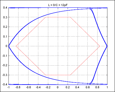
Figure 2. Shows the eye pattern achieved by the MAX4906EF with 12pF capacitance and no series inductor.
The system "passes" but just barely. The left-hand side just barely passes Point 1. The apparently slow rise time is the time the signal takes to go from 50% to 100%; the fall time (the right side) is the time it takes to go from 0 to 50% (much faster). The x-axis is one UI or 2083ps. Point 1 on the diagram is 0.375 UI or 780ps from the beginning of the eye. It must be > 300mV or 75% in amplitude at this point. If the board has a bit too much capacitance, or the device is 15pF instead of 12pF, then the system will fail. The next simulation, shown in Figure 3, adds 18nH in series with device.
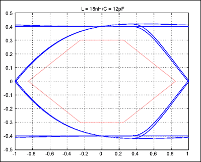
Figure 3. Illustrates the eye pattern for the MAX4906EF with 18nH in series with the device.
With 18nH in series with the MAX4906EF, the difficult Point 1 has much more clearance. High-frequency peaking is evident with 18nH, and the signal is a little higher than might have been expected. For optimal performance, the designer may want to experiment with inductance values between 10nH and 20nH, depending on the board used.

Figure 4. Provides a full schematic of the circuit used to achieve USB 2.0 compliance. This circuit was built and tested; the improvement was evident and correlated very well with the simulation results.
Conclusions
Broadband high-frequency circuits can encounter problems in trying to meet the needs of real-world designs. Inappropriate board traces can add capacitance, compounding the problems and compromising the performance of USB systems.
This application note details a circuit for implementing a USB 2.0-compliant* switched system using the MAX4906EF. The addition of inductors in series with the board traces can peak the high-frequency response at very minimal cost. The nature of the circuit is such that the exact value of the inductor is not very critical, and values ±20% are fine. The system designer is free to add actual physical inductors, or to add spiral traces to the board to achieve the required inductance, which would add no additional cost to the system. The MAX4906EF adds a 2:1 switch to the USB design at near-zero added current, thus enabling a single transceiver to be used for several sockets. The solution is an ultra-low-power, low-cost, two-port implementation of USB 2.0.
*This application note describes how to improve the frequency response of a switch to meet the eye diagram specifications of USB 2.0. However, whether or not the switched system complies with the USB 2.0 specification depends on the system architecture.
Related to this Article
Products
Latest Media 21


