Improving Gain Flatness without Sacrificing Dynamic Performance in High-IF ADCs
Abstract
The article instructs the user how to select the appropriate transformer, typically used in signal-conditioning circuits preceding high-speed analog-to-digital converters (ADCs). The article also explains how to choose passive components to achieve gain flatness over a wide range of input frequencies, without sacrificing the dynamic performance of these ADCs. Finally, the article describes the differences between primary- and secondary-side termination of the transformer, and details their impact on the gain flatness and dynamic range of high-speed ADCs designed for medium- to high-IF applications.
The circuits discussed here convert a single-ended signal, which typically originates from a buffered demodulator circuit, to a differential signal to be fed to the high-IF ADC. These circuits use a wide-band transformer, termination resistors, and filter capacitors to accomplish this task. Also discussed is the best termination scheme for the transformer to maintain a high-speed ADC's high dynamic range, while minimizing the effects of gain peaking and bandwidth reduction.
Single-Ended-to-Differential Conversion with a 200MHz Transformer
The MAX1449 was chosen for demonstration and analysis of two potential input configurations. Figure 1 shows a typical, AC-coupled, single-ended-to-differential conversion design using a wide-band transformer, such as the T1-1T-KK81 (200MHz) from Mini-Circuits®, which has 50Ω primary-side termination and a 25Ω/22pF filter network. In this configuration, a single-ended signal from a 50Ω impedance source is converted to a differential signal through the transformer. Primary-side termination into 50Ω allows excellent matching between the signal source and the transformer. However, this also means that there is a mismatch between the primary and the secondary sides of the transformer. The primary side looks into a combined impedance of 25Ω, while the secondary side experiences a large impedance mismatch with the 20kΩ input resistance of the ADC shunted by 22pF. This impacts the frequency response of the input network, ultimately affecting the frequency response of the converter. The transformer's nominal leakage inductance can range from 25nH to 100nH. Combined with an input filter capacitor of 22pF, this creates a disturbing resonance frequency
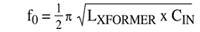
occurring between 110MHz and 215MHz, which results in undesirable gain peaking in this frequency range.
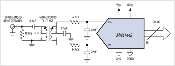
Figure 1. A single-ended signal from a 50Ω-impedance source is taken and converted to a differential signal through a 200MHz transformer.
Single-Ended-to-Differential Conversion with an 800MHz Transformer
Figure 2 depicts a similar AC-coupled configuration. However, this circuit was designed with a better performing wide-band transformer, such as Mini-Circuits' ADT1-1WT (800MHz), which includes a primary-side termination and a 25Ω/10pF filter network. Although, this transformer has an impedance of 75Ω, its lower leakage inductance yields a significantly better frequency response of -1dB up to 400MHz, compared to only 50MHz for the T1-1T-KK81.
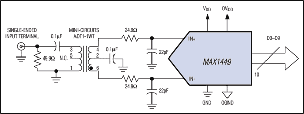
Figure 2. Similar to Figure 1, a single-ended signal is converted to a differential signal. However, this instance occurs through an 800MHz transformer, providing better performance.
Transformers - 200MHz vs. 800MHz
Figure 3 shows the results for both termination schemes and selected filter network components and transformers. A significant improvement can be observed between the two graph plots. The input bandwidth plot for the T1-1T-KK81 transformer clearly shows a gain peaking of about 0.5dB between 90MHz and 110MHz, while the plot for the ADT1-1WT transformer remains flat within 0.1dB for frequencies up to 300MHz. The dynamic performance for this condition (ADT1-1WT transformer, 50Ω primary-side termination, and 10pF input filter capacitors at INP and INN) still yields an excellent SNR of 58.4dB for fIN = 50MHz. Though Figure 3 only displays tested input frequencies of 80MHz and 260MHz (ADT1-1WT only), lab tests have proven that the gain remains flat within 0.1dB to input frequencies well beyond the 8th Nyquist region.
Figure 3. This graph illustrates the significant improvement in gain flatness obtained by using an 800MHz transformer vs. a 200MHz transformer.
Matching the secondary-side impedance of the transformer can help to further enhance gain flatness. One way to do this is by using a secondary-side termination rather than a primary-side termination.
Particularly for high-IF applications, the location of the termination impedance is very important. Depending on the requirements for gain flatness and dynamic performance, an AC-coupled input signal can be terminated on either side of the transformer. Wide-band transformers are popular components that support a fast and easy way to convert a single-ended signal to a differential signal over a wide range of frequencies.
Primary-Side Termination
The MAX1124 (10-bit, 250Msps) was selected to demonstrate different termination schemes and their impact on gain bandwidth and dynamic performance of the ADC. Starting with a primary-side termination configuration (Figure 4a), a 50Ω impedance source signal is applied to means two 25Ω resistors are placed between the top/bottom and center taps of the transformer (Figure 5a). Followed by 0.1µF capacitors for AC-coupling purposes and an input filter network (15Ω series resistor and input impedance of the ADC), a well-balanced secondary-side signal is now applied to the converter. As with the configuration in Figure 4a, no additional input filter capacitors are installed on INP and INN. With this configuration, frequency peaking in the range of 450MHz to 550MHz can be completely eliminated. If required, more DC attenuation can be added by exchanging the 15Ω isolation resistors for 30Ω resistors. Although this approach makes the frequency response smoother, it causes a loss in frequency bandwidth (Figure 5b).
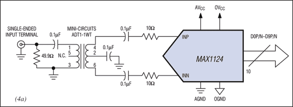
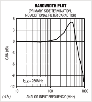
Figure 4. The well-balanced primary side of the transformer in this primary-side termination configuration (Figure 4a) is offset by an imbalance on the secondary side, producing maximum frequency peaking between 450MHz and 550MHz (Figure 4b).
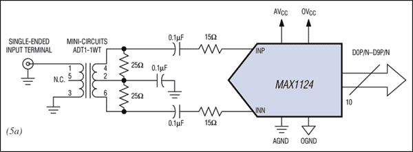
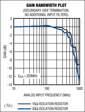
Figure 5. A well-balanced secondary-side signal is applied to the converter (Figure 5a), completely eliminating frequency peaking in the 450MHz to 550MHz range. DC attenuation can be increased, making frequency response smoother, but this will cause loss in frequency bandwidth (Figure 5b).
Conclusion
This article shows that not only the proper choice of passive components plays an important role in designing input networks for high-speed data converters, but the proper use of these components is significant as well. For instance, if gain flatness is an important factor in a system, care must be taken to avoid imbalances and resonances at the differential inputs of the converter to ensure that its true dynamic performance can be replicated. That both configurations do not use input filter capacitors might raise some concern about the impact of additional noise pickup at INP and INN. A brief analysis of this showed a degradation of the signal-to-noise ratio (SNR) between 0.2dB to 0.5dB. As long as wide bandwidth and stability over a wide range of frequencies (gain flatness) and a high dynamic performance are desired, most high- IF applications will accept this rather minor degradation in noise performance for a 10-bit data converter.
Related to this Article
Products
PRODUCTION
1.8V, 10-Bit, 250Msps Analog-to-Digital Converter with LVDS Outputs fo...
LAST TIME BUY
10-Bit, 105Msps, Single +3.3V, Low-Power ADC with Internal Reference
Product Categories
Latest Media 21


